Application-specific integrated circuit
This article includes a list of general references, but it lacks sufficient corresponding inline citations. (October 2015) |


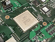
An application-specific integrated circuit (ASIC
As feature sizes have shrunk and
History
Early ASICs used
A successful commercial application of gate array circuitry was found in the low-end 8-bit ZX81 and ZX Spectrum personal computers, introduced in 1981 and 1982. These were used by Sinclair Research (UK) essentially as a low-cost I/O solution aimed at handling the computer's graphics.
Customization occurred by varying a metal interconnect mask. Gate arrays had complexities of up to a few thousand gates; this is now called
Standard-cell designs
In the mid-1980s, a designer would choose an ASIC manufacturer and implement their design using the design tools available from the manufacturer. While third-party design tools were available, there was not an effective link from the third-party design tools to the
By the late 1990s, logic synthesis tools became available. Such tools could compile HDL descriptions into a gate-level netlist. Standard-cell integrated circuits (ICs) are designed in the following conceptual stages referred to as electronics design flow, although these stages overlap significantly in practice:
- Requirements engineering: A team of design engineers starts with a non-formal understanding of the required functions for a new ASIC, usually derived from requirements analysis.
- Register-transfer level (RTL) design: The design team constructs a description of an ASIC to achieve these goals using a hardware description language. This process is similar to writing a computer program in a high-level language.
- test coverage.
- Logic synthesis: standard-cell library consisting of pre-characterized collections of logic gates performing specific functions. The standard cells are typically specific to the planned manufacturer of the ASIC. The resulting collection of standard cells and the needed electrical connections between them is called a gate-level netlist.
- Placement: The gate-level netlist is next processed by a placement tool which places the standard cells onto a region of an integrated circuit die representing the final ASIC. The placement tool attempts to find an optimizedplacement of the standard cells, subject to a variety of specified constraints.
- Routing: An electronics globally optimal" solution. The output is a file which can be used to create a set of photomasks enabling a semiconductor fabrication facility, commonly called a 'fab' or 'foundry' to manufacture physical integrated circuits. Placement and routing are closely interrelated and are collectively called place and routein electronics design.
- Sign-off: Given the final layout, chip fabrication.
These steps, implemented with a level of skill common in the industry, almost always produce a final device that correctly implements the original design, unless flaws are later introduced by the physical fabrication process.[7]
The design steps also called
Gate-array and semi-custom design

Gate-array ASICs are always a compromise between rapid design and
Pure, logic-only gate-array design is rarely implemented by circuit designers today, having been almost entirely replaced by field-programmable devices. The most prominent of such devices are field-programmable gate arrays (FPGAs) which can be programmed by the user and thus offer minimal tooling charges, non-recurring engineering, only marginally increased piece part cost, and comparable performance.
Today, gate arrays are evolving into
In their frequent usages in the field, the terms "gate array" and "semi-custom" are synonymous when referring to ASICs. Process engineers more commonly use the term "semi-custom", while "gate-array" is more commonly used by logic (or gate-level) designers.
Full-custom design

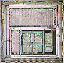
By contrast, full-custom ASIC design defines all the photolithographic layers of the device.[6] Full-custom design is used for both ASIC design and for standard product design.
The benefits of full-custom design include reduced area (and therefore recurring component cost), performance improvements, and also the ability to integrate analog components and other pre-designed—and thus fully verified—components, such as microprocessor cores, that form a system on a chip.
The disadvantages of full-custom design can include increased manufacturing and design time, increased non-recurring engineering costs, more complexity in the computer-aided design (CAD) and electronic design automation systems, and a much higher skill requirement on the part of the design team.
For digital-only designs, however, "standard-cell" cell libraries, together with modern CAD systems, can offer considerable performance/cost benefits with low risk. Automated layout tools are quick and easy to use and also offer the possibility to "hand-tweak" or manually optimize any performance-limiting aspect of the design.
This is designed by using basic logic gates, circuits or layout specially for a design.
Structured design
Structured ASIC design (also referred to as "platform ASIC design") is a relatively new trend in the semiconductor industry, resulting in some variation in its definition. However, the basic premise of a structured ASIC is that both manufacturing cycle time and design cycle time are reduced compared to cell-based ASIC, by virtue of there being pre-defined metal layers (thus reducing manufacturing time) and pre-characterization of what is on the silicon (thus reducing design cycle time).
Definition from Foundations of Embedded Systems states that:[8]
In a "structured ASIC" design, the logic mask-layers of a device are predefined by the ASIC vendor (or in some cases by a third party). Design differentiation and customization is achieved by creating custom metal layers that create custom connections between predefined lower-layer logic elements. "Structured ASIC" technology is seen as bridging the gap between field-programmable gate arrays and "standard-cell" ASIC designs. Because only a small number of chip layers must be custom-produced, "structured ASIC" designs have much smaller non-recurring expenditures (NRE) than "standard-cell" or "full-custom" chips, which require that a full mask set be produced for every design.
— Foundations of Embedded Systems
This is effectively the same definition as a gate array. What distinguishes a structured ASIC from a gate array is that in a gate array, the predefined metal layers serve to make manufacturing turnaround faster. In a structured ASIC, the use of predefined metallization is primarily to reduce cost of the mask sets as well as making the design cycle time significantly shorter.
For example, in a cell-based or gate-array design the user must often design power, clock, and test structures themselves. By contrast, these are predefined in most structured ASICs and therefore can save time and expense for the designer compared to gate-array based designs. Likewise, the design tools used for structured ASIC can be substantially lower cost and easier (faster) to use than cell-based tools, because they do not have to perform all the functions that cell-based tools do. In some cases, the structured ASIC vendor requires customized tools for their device (e.g., custom physical synthesis) be used, also allowing for the design to be brought into manufacturing more quickly.
Cell libraries, IP-based design, hard and soft macros
What most engineers understand as "
Indeed, the wide range of functions now available in structured ASIC design is a result of the phenomenal improvement in electronics in the late 1990s and early 2000s; as a core takes a lot of time and investment to create, its re-use and further development cuts product cycle times dramatically and creates better products. Additionally, open-source hardware organizations such as OpenCores are collecting free IP cores, paralleling the open-source software movement in hardware design.
Soft macros are often process-independent (i.e. they can be fabricated on a wide range of manufacturing processes and different manufacturers). Hard macros are process-limited and usually further design effort must be invested to migrate (port) to a different process or manufacturer.
Multi-project wafers
Some manufacturers and IC design houses offer multi-project wafer service (MPW) as a method of obtaining low cost prototypes. Often called shuttles, these MPWs, containing several designs, run at regular, scheduled intervals on a "cut and go" basis, usually with limited liability on the part of the manufacturer. The contract involves delivery of bare dies or the assembly and packaging of a handful of devices. The service usually involves the supply of a physical design database (i.e. masking information or pattern generation (PG) tape). The manufacturer is often referred to as a "silicon foundry" due to the low involvement it has in the process.
Application-specific standard product

An application-specific standard product or ASSP is an integrated circuit that implements a specific function that appeals to a wide market. As opposed to ASICs that combine a collection of functions and are designed by or for one customer, ASSPs are available as off-the-shelf components. ASSPs are used in all industries, from automotive to communications.[citation needed] As a general rule, if you can find a design in a data book, then it is probably not an ASIC, but there are some exceptions.[clarification needed]
For example, two ICs that might or might not be considered ASICs are a controller chip for a PC and a chip for a modem. Both of these examples are specific to an application (which is typical of an ASIC) but are sold to many different system vendors (which is typical of standard parts). ASICs such as these are sometimes called application-specific standard products (ASSPs).
Examples of ASSPs are encoding/decoding chip, Ethernet network interface controller chip, etc.
See also
- Application-specific instruction set processor (ASIP)
- Complex programmable logic device (CPLD)
- Electronic design automation (EDA or ECAD)
- Field-programmable gate array (FPGA)
- Multi-project chip(MPC)
- Very Large Scale Integration (VLSI)
- System on a chip (SoC)
- Hardware acceleration for an overview of computing based primarily in hardware
References
- ^ OCLC 76935560.
- ^ a b c d "1967: Application Specific Integrated Circuits employ Computer-Aided Design". The Silicon Engine. Computer History Museum. Retrieved 9 November 2019.
- ^ Kriegbaum, Jeff (13 September 2004). "FPGA's vs. ASIC's". EE Times.
- ^ Lipp, Bob oral history. Computer History Museum. 14 February 2017. Retrieved 28 January 2018.
{{cite book}}:|website=ignored (help) - ^ "People". The Silicon Engine. Computer History Museum. Retrieved 28 January 2018.
- ^ ISBN 978-0-201-50022-6.
- OCLC 1132366891.
- S2CID 86596100.
Sources
- Barr, Keith (2007). ASIC Design in the Silicon Sandbox: A Complete Guide to Building Mixed-Signal Integrated Circuits. McGraw Hill Professional. ISBN 978-0-07-148161-8.
- Anthony Cataldo (26 March 2002). "Xilinx looks to ease path to custom FPGAs". EE Times. CMP Media, LLC. Archived from the original on 29 September 2007. Retrieved 14 December 2006.
- "Xilinx intros next-gen EasyPath FPGAs priced below structured ASICs". EDP Weekly's IT Monitor. Millin Publishing, Inc. 18 October 2004.
- Golshan, K. (2007). Physical design essentials: an ASIC design implementation perspective. New York: Springer. ISBN 978-0-387-36642-5.
External links
 Media related to Application-specific integrated circuits at Wikimedia Commons
