
Atomic layer deposition
Atomic layer deposition (ALD) is a
Introduction
During atomic layer deposition, a film is grown on a substrate by exposing its surface to alternate gaseous species (typically referred to as precursors or reactants). In contrast to chemical vapor deposition, the precursors are never present simultaneously in the reactor, but they are inserted as a series of sequential, non-overlapping pulses. In each of these pulses the precursor molecules react with the surface in a self-limiting way, so that the reaction terminates once all the available sites on the surface are consumed. Consequently, the maximum amount of material deposited on the surface after a single exposure to all of the precursors (a so-called ALD cycle) is determined by the nature of the precursor-surface interaction.[1][2] By varying the number of cycles it is possible to grow materials uniformly and with high precision on arbitrarily complex and large substrates.

ALD is a deposition method with great potential for producing very thin, conformal films with control of the thickness and composition of the films possible at the atomic level. A major driving force for the recent interest is the prospective seen for ALD in scaling down microelectronic devices according to Moore's law. ALD is an active field of research, with hundreds of different processes published in the scientific literature,[1][2][4] though some of them exhibit behaviors that depart from that of an ideal ALD process.[4] Currently there are several comprehensive review papers that give a summary of the published ALD processes, including the work of Puurunen,[5] Miikkulainen et al.,[4] Knoops et al.,[6] and Mackus & Schneider et al..[7] An interactive, community driven database of ALD processes is also available online[3] which generates an up-to-date overview in the form of an annotated periodic table.
The sister technique of atomic layer deposition, molecular layer deposition (MLD), uses organic precursors to deposit polymers. By combining the ALD/MLD techniques, it is possible to make highly conformal and pure hybrid films for many applications.
Another technology related to ALD is sequential infiltration synthesis (SIS) which uses alternating precursor vapor exposures to infiltrate and modify polymers. SIS is also referred to as vapor phase infiltration (VPI) and sequential vapor infiltration (SVI).
History
60s
In the 1960s, Stanislav Koltsov together with
In 1974, when starting the development of thin-film
The developers of ML and ALE met at the 1st international conference on atomic layer epitaxy, "ALE-1" in Espoo, Finland, 1990.[10][8] An attempt to expose the extent of molecular layering works was made in a scientific ALD review article in 2005[2] and later in the VPHA-related publications.[14][8][15]
The name "atomic layer deposition" was apparently proposed for the first time in writing as an alternative to ALE in analogy with CVD by Markku Leskelä (professor at the University of Helsinki) at the ALE-1 conference, Espoo, Finland. It took about a decade before the name gained general acceptance with the onset of the international conference series on ALD by American Vacuum Society.[16]
00s
In 2000,
ALD has been developed in two independent discoveries under names atomic layer epitaxy (ALE, Finland) and molecular layering (ML, Soviet Union).[14] To clarify the early history, the Virtual Project on the History of ALD (VPHA) has been set up in summer 2013.[20] it resulted in several publications reviewing the historical development of ALD under the names ALE and ML.[14][10][8][15]
2010s
In 2010, sequential infiltration synthesis (SIS), first reported by researchers at Argonne National Laboratory, was added to the family of ALD-derived techniques.
Surface reaction mechanisms
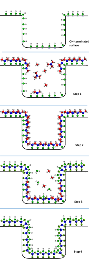
In a prototypical ALD process, a substrate is exposed to two reactants A and B in a sequential, non-overlapping way. In contrast to other techniques such as chemical vapor deposition (CVD), where thin-film growth proceeds on a steady-state fashion, in ALD each reactant reacts with the surface in a self-limited way: the reactant molecules can react only with a finite number of reactive sites on the surface. Once all those sites have been consumed in the reactor, the growth stops. The remaining reactant molecules are flushed away and only then reactant B is inserted into the reactor. By alternating exposures of A and B, a thin film is deposited. This process is shown in the side figure. Consequently, when describing an ALD process one refers to both dose times (the time a surface is being exposed to a precursor) and purge times (the time left in between doses for the precursor to evacuate the chamber) for each precursor. The dose-purge-dose-purge sequence of a binary ALD process constitutes an ALD cycle. Also, rather than using the concept of growth rate, ALD processes are described in terms of their growth per cycle.[21]
In ALD, enough time must be allowed in each reaction step so that a full adsorption density can be achieved. When this happens the process has reached saturation. This time will depend on two key factors: the precursor pressure, and the sticking probability.[22] Therefore, the rate of adsorption per unit of surface area can be expressed as:

Where R is the rate of adsorption, S is the sticking probability, and F is the incident molar flux.[23] However, a key characteristic of ALD is the S will change with time, as more molecules have reacted with the surface this sticking probability will become smaller until reaching a value of zero once saturation is reached.
The specific details on the reaction mechanisms are strongly dependent on the particular ALD process. With hundreds of process available to deposit oxide, metals, nitrides, sulfides, chalcogenides, and fluoride materials,[4] the unraveling of the mechanistic aspects of ALD processes is an active field of research.[24] Some representative examples are shown below.
Thermal ALD

Thermal ALD requires temperatures ranging from room temperature (~20°C) to 350°C for ligand exchange or combustion type surface reactions.[25] It occurs through surface reactions, which enables accurate thickness control no matter the substrate geometry (subject to aspect ratio) and reactor design.[1]
The synthesis of Al2O3 from
Plasma ALD
In plasma-assisted ALD (PA-ALD), the high reactivity of the plasma species allows to reduce the deposition temperature without compromising the film quality; also, a wider range of precursors can be used and thus a wider range of materials can be deposited as compared to thermal ALD.[1]
Spatial ALD
In temporal ALD the separate precursor and co-reactant doses are separated from each other in time by a purge step. In contrast, in spatial ALD (s-ALD), these gases are delivered at different locations, so they are separated in space. In atmospheric pressure s-ALD the precursor and co-reactant are delivered continuously and they are separated from each other by a gas curtain to prevent gas phase reactions. Such gas curtain typically consists of nitrogen injection and exhaust positions, see Figure 1. As a substrates moves through the different gas zones, self-limiting reactions take place at the substrate surface and the ALD process takes place. As this process can easily be accelerated, the deposition rate for spatial ALD can be much higher than for conventional ALD. For example, for ALD of Al2O3 the deposition rate increases from 100-300 nm per hour to 60 nm per minute.[5]

The inline nature of spatial ALD makes it suitable for high volume production lines and roll-to-roll production. In general, s-ALD has been employed to apply moisture permeation barriers, passivation layers in silicon solar cells and functional layers in batteries. The chemistry for spatial ALD processes is comparable with typical temporal ALD processes, and materials that have been explored include inorganic metal oxides such as Al2O3, (Al- or Ga doped) ZnO, SiO2, In2O3, InZnO, LIPON, Zn(O,S), SnOx, and TiOx ,but also PMG metals (Pt, Ir, Ru) can be deposited. Additionally, organic molecules can be grown in combination with inorganic atoms to enable molecular layer deposition (MLD). Plasma- or ozon enhanced spatial ALD has been demonstrated which generally lowers the deposition temperatures required.
Photo-assisted ALD
In this ALD variety, UV light is used to accelerate surface reactions on the substrate. Hence reaction temperature can be reduced, as in plasma-assisted ALD. As compared to plasma-assisted ALD, the activation is weaker, but is often easier to control by adjusting the wavelength, intensity and timing of illumination.[1]
Metal ALD
Copper metal ALD has attracted much attention due to the demand for copper as an
Some metals can be grown by ALD via fluorosilane elimination reactions using a metal halide and a silicon precursor (e.g. SiH4, Si2H6) as the reactants. These reactions are very exothermic due to the formation of stable Si–F bonds.[24] Metals deposited by fluorosilane elimination include tungsten[31] and molybdenum.[32] As an example, the surface reactions for tungsten metal ALD using WF6 and Si2H6 as the reactants can be expressed as[31][33]
- WSiF2H* + WF6 → WWF5* + SiF3H
- WF5* + Si2H6 → WSiF2H* + SiF3H + 2 H2
The overall ALD reaction is[24]
- WF6 + Si2H6 → W + SiF3H + 2 H2, ∆H = –181 kcal
The growth rate can vary from 4 to 7 Å/cycle depending on the deposition temperature (177 to 325 °C) and Si2H6 reactant exposure (~104 to 106 L), factors that may influence Si2H6 insertion into Si–H bonds[34][35] and result in a silicon CVD contribution to the tungsten ALD growth.[24]
The thermal ALD of many other metals is challenging (or presently impossible) due to their very negative electrochemical potentials. Recently, the application of novel strong
Catalytic SiO2 ALD
The use of catalysts is of paramount importance in delivering reliable methods of SiO2 ALD. Without
- Primary reactions at surface:
- SiOH* + SiCl4 → SiOSiCl3* + HCl
- SiCl* + H2O → SiOH* + HCl
- Overall ALD reaction:
- SiCl4 + 2H2O → SiO2 + 4 HCl

| Type of ALD | Temperature range | Viable precursors | Reactants | Applications |
|---|---|---|---|---|
| Catalytic ALD | >32 °C with Lewis base catalyst[24] | Metal oxides (i.e. TiO2, ZrO2,SnO2)[24] | (Metal)Cl4, H2O[24] | High k-dielectric layers, protective layers, anti-reflective layers, etc.[24] |
| Al2O3 ALD | 30–300 °C | Al2O3, metal oxides[41] | (Metal)Cl4, H2O, Ti(OiPr)4, (Metal)(Et)2[24] | Dielectric layers, insulating layers, etc., Solar Cell surface passivations[41] |
| Metal ALD using thermal chemistry | 175–400 °C[42] | Metal Fluorides, organometallics, catalytic metals[42] | M(C5H5)2, (CH3C5H4)M(CH3)3 ,Cu(thd)2, Pd(hfac)2, Ni(acac)2, H2[42] | Conductive pathways, catalytic surfaces, MOS devices[42] |
| ALD on polymers | 25–100 °C[24] | Common polymers (polyethylene, PMMA, PP, PS, PVC, PVA, etc.)[24] | Al(CH3)3, H2O, M(CH3)3[24] | Polymer surface functionalization, creation of composites, diffusion barriers, etc.[24] |
| ALD on particles | 25–100 °C for polymer particles, 100–400 °C for metal/alloy particles[24] | BN, ZrO2, CNTs, polymer particles | Various gases: Fluidized bed reactors are used to allow coating of individual particles[24] | Deposition of protective and insulative coatings, optical and mechanical property modification, formation of composite structures, conductive mediums |
| Plasma or radical-enhanced ALD for single element ALD materials | 20–800 °C[43][24] | Pure metals (i.e. Ta, Ti, Si, Ge, Ru, Pt), metal nitrides (i.e. TiN, TaN, etc.)[24] | Organometallics, MH2Cl2, tertbutylimidotris(diethylamido)tantalum (TBTDET), bis(ethylcyclopentadienyl)ruthenium), NH3[24] | DRAM structures, MOSFET and semiconductor devices, capacitors[44] |
| Plasma-enhanced ALD of metal oxides and nitrides | 20–300 °C | Al2O3, SiO2, ZnOx, InOx, HfO2, SiNx, TaNx[45][46][47] | Similar to thermal ALD |
Applications
Microelectronics applications
ALD is a useful process for the fabrication of microelectronics due to its ability to produce accurate thicknesses and uniform surfaces in addition to high quality film production using various different materials. In microelectronics, ALD is studied as a potential technique to deposit
Gate oxides
Deposition of the
Transition-metal nitrides
Transition-metal
Metal films
Motivations of an interest in metal ALD are:
- Cu interconnects and W plugs, or at least Cu seed layers[49]for Cu electrodeposition and W seeds for W CVD,
- transition-metal nitrides (e.g. TiN, TaN, WN) for Cu interconnect barriers
- noble metals for ferroelectric random access memory (FRAM) and DRAM capacitor electrodes
- high- and low-work function metals for dual-gate MOSFETs.
Magnetic recording heads
Magnetic recording heads utilize electric fields to polarize particles and leave a magnetized pattern on a hard disk.[50] Al2O3 ALD is used to create uniform, thin layers of insulation.[51] By using ALD, it is possible to control the insulation thickness to a high level of accuracy. This allows for more accurate patterns of magnetized particles and thus higher quality recordings.
DRAM capacitors
DRAM capacitors are yet another application of ALD. An individual DRAM cell can store a single bit of data and consists of a single MOS transistor and a capacitor. Major efforts are being put into reducing the size of the capacitor which will effectively allow for greater memory density. In order to change the capacitor size without affecting the capacitance, different cell orientations are being used. Some of these include stacked or trench capacitors.[52] With the emergence of trench capacitors, the problem of fabricating these capacitors comes into play, especially as the size of semiconductors decreases. ALD allows trench features to be scaled to beyond 100 nm. The ability to deposit single layers of material allows for a great deal of control over the material. Except for some issues of incomplete film growth (largely due to insufficient amount or low temperature substrates), ALD provides an effective means of depositing thin films like dielectrics or barriers.[53]
Photovoltaic Applications
The use of ALD technique in solar cells is becoming more prominent with time. In the past, it has been used to deposit surface passivation layers in crystalline-silicon (c-Si) solar cells, buffer layers in copper indium gallium selenide (CIGS) solar cells and barrier layers in dye-sensitized solar cells (DSSCs).[54] For e.g., the use of ALD grown Al2O3 for solar cell applications was demonstrated by Schmidt et al. It was used as a surface passivation layer for the development of PERC (passivated emitter and rear cell) solar cells.[55] The use of ALD technique to deposit charge transport layers (CTLs) is also being explored widely for perovskite solar cells. The ability of ALD to deposit high quality and conformal films with precise control on thickness can provide great advantage in finely tailoring the interfaces between CTL and perovskite layer. Moreover, it can be useful in obtaining uniform and pin-hole free films over large areas. These aspects make ALD a promising technique in further improving and stabilizing the performance of perovskite solar cells.[56]
Electrooptic Applications
Thin Film Couplers
As photonic integrated circuits (PICs) emerge, often in a manner similar to electronic integrated circuits, a wide variety of on-chip optical device structures are needed. One example is the nanophotonic coupler that behaves as a micrometer-size beamsplitter at the intersection of optical waveguides[57] in which high aspect ratio trenches (~100 nm width x 4 micrometer depth) are first defined by etching then back-filled with aluminum oxide by ALD to form optical-quality interfaces.
Biomedical applications
Understanding and being able to specify the surface properties on
Some current uses in biomedical applications include creating flexible sensors, modifying nanoporous membranes, polymer ALD, and creating thin biocompatible coatings. ALD has been used to deposit TiO2 films to create optical waveguide sensors as diagnostic tools.[59] Also, ALD is beneficial in creating flexible sensing devices that can be used, for example, in the clothing of athletes to detect movement or heart rate. ALD is one possible manufacturing process for flexible organic field-effect transistors (OFETs) because it is a low-temperature deposition method.[60]
Nanoporous materials are emerging throughout the biomedical industry in drug delivery, implants, and tissue engineering. The benefit of using ALD to modify the surfaces of nanoporous materials is that, unlike many other methods, the saturation and self-limiting nature of the reactions means that even deeply embedded surfaces and interfaces are coated with a uniform film.[1] Nanoporous surfaces can have their pore size reduced further in the ALD process because the conformal coating will completely coat the insides of the pores. This reduction in pore size may be advantageous in certain applications.[61]
As a permeation barrier for plastics
ALD can be used as a permeation barrier for plastics.[62] For example, it is well established as a method for encapsulation of OLEDs on plastic.[63][64] ALD can also be used to inoculate 3-D printed plastic parts for use in vacuum environments by mitigating outgassing, which allows for custom low-cost tools for both semiconductor processing and space applications.[65] ALD can be used to form a barrier on plastics in roll to roll processes.[66]
Quality and its control
The quality of an ALD process can be monitored using several different imaging techniques to make sure that the ALD process is occurring smoothly and producing a conformal layer over a surface. One option is the use of cross-sectional scanning electron microscopy (SEM) or transmission electron microscopy (TEM). High magnification of images is pertinent for assessing the quality of an ALD layer. X-ray reflectivity (XRR) is a technique that measures thin-film properties including thickness, density, and surface roughness.[67] Another optical quality evaluation tool is spectroscopic ellipsometry. Its application between the depositions of each layer by ALD provides information on the growth rate and material characteristics of the film.[68]
Applying this analysis tool during the ALD process, sometimes referred to as in situ spectroscopic
Advantages and limitations
Advantages
ALD provides a very controlled method to produce a film to an atomically specified thickness. Also, the growth of different multilayer structures is straightforward. Because of the sensitivity and precision of the equipment, it is very beneficial to those in the field of microelectronics and nanotechnology in producing small, but efficient semiconductors. ALD typically involves the use of relatively low temperatures and a catalyst, which is thermochemically favored. The lower temperature is beneficial when working with soft substrates, such as organic and biological samples. Some precursors that are thermally unstable still may be used so long as their decomposition rate is relatively slow.[1][24]
Disadvantages
High purity of the substrates is very important, and as such, high costs will ensue. Although this cost may not be much relative to the cost of the equipment needed, one may need to run several trials before finding conditions that favor their desired product. Once the layer has been made and the process is complete, there may be a requirement of needing to remove excess precursors from the final product. In some final products there are less than 1% of impurities present.[69]
Economic viability
Atomic layer deposition instruments can range anywhere from $200,000 to $800,000 based on the quality and efficiency of the instrument. There is no set cost for running a cycle of these instruments; the cost varies depending on the quality and purity of the substrates used, as well as the temperature and time of machine operation. Some substrates are less available than others and require special conditions, as some are very sensitive to oxygen and may then increase the rate of decomposition. Multicomponent oxides and certain metals traditionally needed in the microelectronics industry are generally not cost efficient.[70]
Reaction time
The process of ALD is very slow and this is known to be its major limitation. For example, Al2O3 is deposited at a rate of 0.11 nm per cycle,[2] which can correspond to an average deposition rate of 100–300 nm per hour, depending on cycle duration and pumping speed. This problem can be overrun by using Spatial ALD, where the substrate is moved in space below a special ALD showerhead, and both the precursor gasses are separated by gas curtains/bearings. In this way, deposition rates of 60 nm per minute could be reached. ALD is typically used to produce substrates for microelectronics and nanotechnology, and therefore, thick atomic layers are not needed. Many substrates cannot be used because of their fragility or impurity. Impurities are typically found on the 0.1–1 at.% because of some of the carrier gases are known to leave residue and are also sensitive to oxygen.[69]
Chemical limitations
Precursors must be volatile, but not subject to decomposition, as most precursors are very sensitive to oxygen/air, thus causing a limitation on the substrates that may be used. Some biological substrates are very sensitive to heat and may have fast decomposition rates that are not favored and yield larger impurity levels. There are a multitude of thin-film substrate materials available, but the important substrates needed for use in microelectronics can be hard to obtain and may be very expensive.[69]
References
- ^ PMID 31164953.

- ^ .
- ^ .
- ^ .
- ^ .
- S2CID 108003079.
- S2CID 104385650.
- ^ .
- ^ Aleskovskii, V. B. Zh. Prikl. Khim. 47, 2145 (1974); [J. Appl. Chem. USSR. 47, 2207, (1974)].
- ^ S2CID 137543630.
- ^ a b c Suntola, T. and Antson, J. (1977) U.S. patent 4,058,430 "Method for producing compound thin films"
- ^ Suntola, T.; Pakkala, A. and Lindfors, S. (1983) U.S. patent 4,389,973 "Apparatus for performing growth of compound thin films"
- ^ "2018 Millennium Technology Prize for Tuomo Suntola – Finnish physicist's innovation enables manufacture and development of information technology products" (Press release). Technology Academy Finland. 22 May 2018. Retrieved 22 May 2018.
- ^ S2CID 209855960.
- ^ S2CID 240379307. Retrieved 26 December 2018.
- S2CID 97676893.
- ^ "IEEE Andrew S. Grove Award Recipients". IEEE Andrew S. Grove Award. Institute of Electrical and Electronics Engineers. Retrieved 4 July 2019.
- ^ Sandhu, Gurtej; Doan, Trung T. (22 August 2001). "Atomic layer doping apparatus and method". Google Patents. Retrieved 5 July 2019.
- S2CID 12392861. Archived from the original(PDF) on 18 February 2008.
- ^ Virtual project on the history of ALD. vph-ald.com
- ^ "How Atomic Layer Deposition Works". Youtube (2011).
- ISBN 978-3-527-41216-7.
- ^ "2.3 Adsorption Kinetics – The Rate of Adsorption". www.chem.qmul.ac.uk.
- ^ PMID 19947596.
- ^ Güder, Firat (2012). Atomlagenabscheidung unterstützt Nanostrukturelle Transformationen [Atomic layer deposition assisted nanostructural transformations] (Doctoral thesis) (in German). University of Freiburg. Front cover image.
- ^ .
- OCLC 730008390.
- S2CID 97668427.
- ISSN 0897-4756.
- ISSN 0897-4756.
- ^ .
- ISSN 0897-4756.
- .
- .
- .
- PMID 23947400.
- ISSN 0897-4756.
- S2CID 104844454.
- ISSN 0897-4756.
- .
- ^ .
- ^ .
- .
- ^ Greer, Frank; Fraser, D.; Coburn, J.W. and Graves, David B. (2002) "Fundamental Vacuum Beam Studies of Radical Enhanced Atomic Layer Chemical Vapor Deposition (REAL-CVD) of TiN". NCCAVS.
- .
- PMID 26305370.
- .
- .
- .
- ^ Magnetic Recording Theory. stanford.edu
- ^ Leskelä, Markku (2010). "Industrial Applications of Atomic Layer Deposition (ALD)". 10th MIICS Conference. Archived from the original on 30 May 2012.
- ISBN 978-1877750595.
- ^ Gutsche, M. (2003). "Atomic Layer Deposition for Advanced DRAM Applications". Future Fab Intl. 14. Archived from the original on 8 September 2005.
- S2CID 55670928.
- S2CID 97771156.
- S2CID 73448015.
- S2CID 46191619.
- .
- .
- .
- S2CID 135635044.
- S2CID 250740101.
- S2CID 135967211.
- S2CID 58156645.
- S2CID 212841294.
- .
- ^ Yasaka, Miho (2010). "X-ray thin-film measurement techniques" (PDF). The Rigaku Journal. 26 (2): 1–9.
- ^ S2CID 97244909.
- ^ PMID 14639717. Archived from the original(PDF) on 14 July 2014.
- ^ "Molecular Beam Epitaxy & Atomic Layer Deposition Systems". SVT Associates.