
Carbon nanotube

| Part of a series of articles on |
| Nanomaterials |
|---|
 |
| Carbon nanotubes |
| Fullerenes |
| Other nanoparticles |
| Nanostructured materials |
A carbon nanotube (CNT) is a tube made of carbon with a diameter in the nanometre range (
Single-walled carbon nanotubes (SWCNTs) have diameters around 0.5–2.0
Multi-walled carbon nanotubes (MWCNTs) consist of nested single-wall carbon nanotubes[1] in a nested, tube-in-tube structure.[2] Double- and triple-walled carbon nanotubes are special cases of MWCNT.
Carbon nanotubes can exhibit remarkable properties, such as exceptional
The predicted properties for SWCNTs were tantalising, but a path to synthesising them was lacking until 1993, when Iijima and Ichihashi at NEC, and Bethune and others at IBM independently discovered that co-vaporising carbon and transition metals such as iron and cobalt could specifically catalyse SWCNT formation.[13][14] These discoveries triggered research that succeeded in greatly increasing the efficiency of the catalytic production technique,[15] and led to an explosion of work to characterise and find applications for SWCNTs.
Structure of SWNTs


Basic details


The structure of an ideal (infinitely long) single-walled carbon nanotube is that of a regular hexagonal lattice drawn on an infinite cylindrical surface, whose vertices are the positions of the carbon atoms. Since the length of the carbon-carbon bonds is fairly fixed, there are constraints on the diameter of the cylinder and the arrangement of the atoms on it.[16]
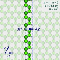
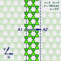
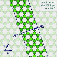
In the study of nanotubes, one defines a zigzag path on a graphene-like lattice as a path that turns 60 degrees, alternating left and right, after stepping through each bond. It is also conventional to define an armchair path as one that makes two left turns of 60 degrees followed by two right turns every four steps. On some carbon nanotubes, there is a closed zigzag path that goes around the tube. One says that the tube is of the zigzag type or configuration, or simply is a zigzag nanotube. If the tube is instead encircled by a closed armchair path, it is said to be of the armchair type, or an armchair nanotube. An infinite nanotube that is of one type consists entirely of closed paths of that type, connected to each other.
The zigzag and armchair configurations are not the only structures that a single-walled nanotube can have. To describe the structure of a general infinitely long tube, one should imagine it being sliced open by a cut parallel to its axis, that goes through some atom A, and then unrolled flat on the plane, so that its atoms and bonds coincide with those of an imaginary graphene sheet—more precisely, with an infinitely long strip of that sheet. The two halves of the atom A will end up on opposite edges of the strip, over two atoms A1 and A2 of the graphene. The line from A1 to A2 will correspond to the circumference of the cylinder that went through the atom A, and will be perpendicular to the edges of the strip. In the graphene lattice, the atoms can be split into two classes, depending on the directions of their three bonds. Half the atoms have their three bonds directed the same way, and half have their three bonds rotated 180 degrees relative to the first half. The atoms A1 and A2, which correspond to the same atom A on the cylinder, must be in the same class. It follows that the circumference of the tube and the angle of the strip are not arbitrary, because they are constrained to the lengths and directions of the lines that connect pairs of graphene atoms in the same class.
Let u and v be two
Types
The structure of the nanotube is not changed if the strip is rotated by 60 degrees clockwise around A1 before applying the hypothetical reconstruction above. Such a rotation changes the corresponding pair (n,m) to the pair (−2m,n+m). It follows that many possible positions of A2 relative to A1 — that is, many pairs (n,m) — correspond to the same arrangement of atoms on the nanotube. That is the case, for example, of the six pairs (1,2), (−2,3), (−3,1), (−1,−2), (2,−3), and (3,−1). In particular, the pairs (k,0) and (0,k) describe the same nanotube geometry. These redundancies can be avoided by considering only pairs (n,m) such that n > 0 and m ≥ 0; that is, where the direction of the vector w lies between those of u (inclusive) and v (exclusive). It can be verified that every nanotube has exactly one pair (n,m) that satisfies those conditions, which is called the tube's type. Conversely, for every type there is a hypothetical nanotube. In fact, two nanotubes have the same type if and only if one can be conceptually rotated and translated so as to match the other exactly. Instead of the type (n,m), the structure of a carbon nanotube can be specified by giving the length of the vector w (that is, the circumference of the nanotube), and the angle α between the directions of u and w, may range from 0 (inclusive) to 60 degrees clockwise (exclusive). If the diagram is drawn with u horizontal, the latter is the tilt of the strip away from the vertical.


Chirality and mirror symmetry
A nanotube is
Circumference and diameter
From n and m one can also compute the circumference c, which is the length of the vector w, which turns out to be:

in picometres. The diameter of the tube is then , that is


also in picometres. (These formulas are only approximate, especially for small n and m where the bonds are strained; and they do not take into account the thickness of the wall.)
The tilt angle α between u and w and the circumference c are related to the type indices n and m by:

where arg(x,y) is the clockwise angle between the X-axis and the vector (x,y); a function that is available in many programming languages as atan2(y,x). Conversely, given c and α, one can get the type (n,m) by the formulas:

which must evaluate to integers.
Physical limits
Narrowest examples

If n and m are too small, the structure described by the pair (n,m) will describe a molecule that cannot be reasonably called a "tube", and may not even be stable. For example, the structure theoretically described by the pair (1,0) (the limiting "zigzag" type) would be just a chain of carbons. That is a real molecule, the carbyne; which has some characteristics of nanotubes (such as orbital hybridization, high tensile strength, etc.) — but has no hollow space, and may not be obtainable as a condensed phase. The pair (2,0) would theoretically yield a chain of fused 4-cycles; and (1,1), the limiting "armchair" structure, would yield a chain of bi-connected 4-rings. These structures may not be realizable.
The thinnest carbon nanotube proper is the armchair structure with type (2,2), which has a diameter of 0.3 nm. This nanotube was grown inside a multi-walled carbon nanotube. Assigning of the carbon nanotube type was done by a combination of high-resolution transmission electron microscopy (HRTEM), Raman spectroscopy, and density functional theory (DFT) calculations.[17]
The thinnest freestanding single-walled carbon nanotube is about 0.43 nm in diameter.[18] Researchers suggested that it can be either (5,1) or (4,2) SWCNT, but the exact type of the carbon nanotube remains questionable.[19] (3,3), (4,3), and (5,1) carbon nanotubes (all about 0.4 nm in diameter) were unambiguously identified using aberration-corrected high-resolution transmission electron microscopy inside double-walled CNTs.[20]
Length

The observation of the longest carbon nanotubes grown so far, around 0.5 metre (550 mm) long, was reported in 2013.[21] These nanotubes were grown on silicon substrates using an improved chemical vapor deposition (CVD) method and represent electrically uniform arrays of single-walled carbon nanotubes.[22]
The shortest carbon nanotube can be considered to be the organic compound cycloparaphenylene, which was synthesized in 2008 by Ramesh Jasti.[23] Other small molecule carbon nanotubes have been synthesized since.[24]
Density
The highest density of CNTs was achieved in 2013, grown on a conductive titanium-coated copper surface that was coated with co-catalysts cobalt and molybdenum at lower than typical temperatures of 450 °C. The tubes averaged a height of 380 nm and a mass density of 1.6 g cm−3. The material showed ohmic conductivity (lowest resistance ~22 kΩ).[25][26]
Variants
There is no consensus on some terms describing carbon nanotubes in the scientific literature: both "-wall" and "-walled" are being used in combination with "single", "double", "triple", or "multi", and the letter C is often omitted in the abbreviation, for example, multi-walled carbon nanotube (MWNT). The
Multi-walled

Multi-walled nanotubes (MWNTs) consist of multiple rolled layers (concentric tubes) of graphene. There are two models that can be used to describe the structures of multi-walled nanotubes. In the
Double-walled carbon nanotubes (DWNTs) form a special class of nanotubes because their
The telescopic motion ability of inner shells
Junctions and crosslinking

Junctions between two or more nanotubes have been widely discussed theoretically.[33][34] Such junctions are quite frequently observed in samples prepared by arc discharge as well as by chemical vapor deposition. The electronic properties of such junctions were first considered theoretically by Lambin et al.,[35] who pointed out that a connection between a metallic tube and a semiconducting one would represent a nanoscale heterojunction. Such a junction could therefore form a component of a nanotube-based electronic circuit. The adjacent image shows a junction between two multiwalled nanotubes.
Junctions between nanotubes and graphene have been considered theoretically[36] and studied experimentally.[37] Nanotube-graphene junctions form the basis of pillared graphene, in which parallel graphene sheets are separated by short nanotubes.[38] Pillared graphene represents a class of three-dimensional carbon nanotube architectures.

Recently, several studies have highlighted the prospect of using carbon nanotubes as building blocks to fabricate three-dimensional macroscopic (>100 nm in all three dimensions) all-carbon devices. Lalwani et al. have reported a novel radical-initiated thermal crosslinking method to fabricate macroscopic, free-standing, porous, all-carbon scaffolds using single- and multi-walled carbon nanotubes as building blocks.[39] These scaffolds possess macro-, micro-, and nano-structured pores, and the porosity can be tailored for specific applications. These 3D all-carbon scaffolds/architectures may be used for the fabrication of the next generation of energy storage, supercapacitors, field emission transistors, high-performance catalysis, photovoltaics, and biomedical devices, implants, and sensors.[40][41]
Other morphologies

Carbon nanobuds are a newly created material combining two previously discovered allotropes of carbon: carbon nanotubes and fullerenes. In this new material, fullerene-like "buds" are covalently bonded to the outer sidewalls of the underlying carbon nanotube. This hybrid material has useful properties of both fullerenes and carbon nanotubes. In particular, they have been found to be exceptionally good field emitters.[42] In composite materials, the attached fullerene molecules may function as molecular anchors preventing slipping of the nanotubes, thus improving the composite's mechanical properties.
A carbon peapod[43][44] is a novel hybrid carbon material which traps fullerene inside a carbon nanotube. It can possess interesting magnetic properties with heating and irradiation. It can also be applied as an oscillator during theoretical investigations and predictions.[45][46]
In theory, a nanotorus is a carbon nanotube bent into a torus (doughnut shape). Nanotori are predicted to have many unique properties, such as magnetic moments 1000 times larger than that previously expected for certain specific radii.[47] Properties such as magnetic moment, thermal stability, etc. vary widely depending on the radius of the torus and the radius of the tube.[47][48]
Graphenated carbon nanotubes are a relatively new hybrid that combines graphitic foliates grown along the sidewalls of multiwalled or bamboo-style CNTs. The foliate density can vary as a function of deposition conditions (e.g., temperature and time) with their structure ranging from a few layers of graphene (< 10) to thicker, more graphite-like.[49] The fundamental advantage of an integrated graphene-CNT structure is the high surface area three-dimensional framework of the CNTs coupled with the high edge density of graphene. Depositing a high density of graphene foliates along the length of aligned CNTs can significantly increase the total charge capacity per unit of nominal area as compared to other carbon nanostructures.[50]
Cup-stacked carbon nanotubes (CSCNTs) differ from other quasi-1D carbon structures, which normally behave as quasi-metallic conductors of electrons. CSCNTs exhibit semiconducting behavior because of the stacking microstructure of graphene layers.[51]
Properties
Many properties of single-walled carbon nanotubes depend significantly on the (n,m) type, and this dependence is non-
Mechanical
Carbon nanotubes are the strongest and stiffest materials yet discovered in terms of
Although the strength of individual CNT shells is extremely high, weak shear interactions between adjacent shells and tubes lead to significant reduction in the effective strength of multiwalled carbon nanotubes and carbon nanotube bundles down to only a few GPa.[54] This limitation has been recently addressed by applying high-energy electron irradiation, which crosslinks inner shells and tubes, and effectively increases the strength of these materials to ≈60 GPa for multiwalled carbon nanotubes[52] and ≈17 GPa for double-walled carbon nanotube bundles.[54] CNTs are not nearly as strong under compression. Because of their hollow structure and high aspect ratio, they tend to undergo buckling when placed under compressive, torsional, or bending stress.[55]
On the other hand, there was evidence that in the radial direction they are rather soft. The first
It was reported in 2020, that CNT-filled polymer nanocomposites with 4 wt% and 6 wt% loadings are the most optimal concentrations, as they provide a good balance between mechanical properties and resilience of mechanical properties against UV exposure for the offshore umbilical sheathing layer.[56]
Electrical

Unlike graphene, which is a two-dimensional semimetal, carbon nanotubes are either metallic or semiconducting along the tubular axis. For a given (n,m) nanotube, if n = m, the nanotube is metallic; if n − m is a multiple of 3 and n ≠ m, then the nanotube is quasi-metallic with a very small band gap, otherwise the nanotube is a moderate semiconductor.[57] Thus, all armchair (n = m) nanotubes are metallic, and nanotubes (6,4), (9,1), etc. are semiconducting.[58] Carbon nanotubes are not semimetallic because the degenerate point (the point where the π [bonding] band meets the π* [anti-bonding] band, at which the energy goes to zero) is slightly shifted away from the K point in the Brillouin zone because of the curvature of the tube surface, causing hybridization between the σ* and π* anti-bonding bands, modifying the band dispersion.
The rule regarding metallic versus semiconductor behavior has exceptions because curvature effects in small-diameter tubes can strongly influence electrical properties. Thus, a (5,0) SWCNT that should be semiconducting in fact is metallic according to the calculations. Likewise, zigzag and chiral SWCNTs with small diameters that should be metallic have a finite gap (armchair nanotubes remain metallic).[58] In theory, metallic nanotubes can carry an electric current density of 4 × 10⁹ A/cm2, which is more than 1,000 times greater than those of metals such as copper,[59] where for copper interconnects, current densities are limited by electromigration. Carbon nanotubes are thus being explored as interconnects and conductivity-enhancing components in composite materials, and many groups are attempting to commercialize highly conducting electrical wire assembled from individual carbon nanotubes. There are significant challenges to be overcome however, such as undesired current saturation under voltage,[60] and the much more resistive nanotube-to-nanotube junctions and impurities, all of which lower the electrical conductivity of the macroscopic nanotube wires by orders of magnitude, as compared to the conductivity of the individual nanotubes.
Because of its nanoscale cross-section, electrons propagate only along the tube's axis. As a result, carbon nanotubes are frequently referred to as one-dimensional conductors. The maximum
Because of the role of the π-electron system in determining the electronic properties of graphene, doping in carbon nanotubes differs from that of bulk crystalline semiconductors from the same group of the periodic table (e.g., silicon). Graphitic substitution of carbon atoms in the nanotube wall by boron or nitrogen dopants leads to p-type and n-type behavior, respectively, as would be expected in silicon. However, some non-substitutional (intercalated or adsorbed) dopants introduced into a carbon nanotube, such as alkali metals and electron-rich metallocenes, result in n-type conduction because they donate electrons to the π-electron system of the nanotube. By contrast, π-electron acceptors such as FeCl3 or electron-deficient metallocenes function as p-type dopants because they draw π-electrons away from the top of the valence band.
Intrinsic superconductivity has been reported,[62][63][64] although other experiments found no evidence of this, leaving the claim a subject of debate.[65]
In 2021, Michael Strano, the Carbon P. Dubbs Professor of Chemical Engineering at MIT, published department findings on the use of carbon nanotubes to create an electric current.[66] By immersing the structures in an organic solvent, the liquid drew electrons out of the carbon particles. Strano was quoted as saying, "This allows you to do electrochemistry, but with no wires," and represents a significant breakthrough in the technology.[67] Future applications include powering micro- or nanoscale robots, as well as driving alcohol oxidation reactions, which are important in the chemicals industry.[67]
Crystallographic defects also affect the tube's electrical properties. A common result is lowered conductivity through the defective region of the tube. A defect in metallic armchair-type tubes (which can conduct electricity) can cause the surrounding region to become semiconducting, and single monatomic vacancies induce magnetic properties.[68]
Optical
Carbon nanotubes have useful absorption, photoluminescence (fluorescence), and Raman spectroscopy properties. Spectroscopic methods offer the possibility of quick and non-destructive characterization of relatively large amounts of carbon nanotubes. There is a strong demand for such characterization from the industrial point of view: numerous parameters of nanotube synthesis can be changed, intentionally or unintentionally, to alter the nanotube quality, such as the non-tubular carbon content, structure (chirality) of the produced nanotubes, and structural defects. These features then determine nearly all other significant optical, mechanical, and electrical properties.
Carbon nanotube optical properties have been explored for use in applications such as for light-emitting diodes (
Thermal
All nanotubes are expected to be very good
Crystallographic defects strongly affect the tube's thermal properties. Such defects lead to phonon scattering, which in turn increases the relaxation rate of the phonons. This reduces the mean free path and reduces the thermal conductivity of nanotube structures. Phonon transport simulations indicate that substitutional defects such as nitrogen or boron will primarily lead to the scattering of high-frequency optical phonons. However, larger-scale defects such as Stone–Wales defects cause phonon scattering over a wide range of frequencies, leading to a greater reduction in thermal conductivity.[82]
Synthesis
Techniques have been developed to produce nanotubes in sizeable quantities, including arc discharge, laser ablation, chemical vapor deposition (CVD) and high-pressure carbon monoxide disproportionation (HiPCO). Among these arc discharge, laser ablation are batch by batch process, Chemical Vapor Deposition can be used both for batch by batch or continuous processes,[83][84] and HiPCO is gas phase continuous process.[85] Most of these processes take place in a vacuum or with process gases. The CVD growth method is popular, as it yields high quantity and has a degree of control over diameter, length and morphology. Using particulate catalysts, large quantities of nanotubes can be synthesized by these methods, and industrialisation is well on its way, with several CNT and CNT fibers factory around the world. One problem of CVD processes is the high variability in the nanotube's characteristics [86] The HiPCO process advances in catalysis and continuous growth are making CNTs more commercially viable.[87] The HiPCO process helps in producing high purity single-walled carbon nanotubes in higher quantity. The HiPCO reactor operates at high temperature 900-1100 °C and high pressure ~30-50 bar.[88] It uses carbon monoxide as the carbon source and iron pentacarbonyl or nickel tetracarbonyl as a catalyst. These catalysts provide a nucleation site for the nanotubes to grow,[85] while cheaper iron-based catalysts like Ferrocene can be used for CVD process.
Vertically aligned carbon nanotube arrays are also grown by thermal chemical vapor deposition. A substrate (quartz, silicon, stainless steel, carbon fibers, etc.) is coated with a catalytic metal (Fe, Co, Ni) layer. Typically that layer is iron and is deposited via sputtering to a thickness of 1–5 nm. A 10–50 nm underlayer of alumina is often also put down on the substrate first. This imparts controllable wetting and good interfacial properties. When the substrate is heated to the growth temperature (~600 to 850 °C), the continuous iron film breaks up into small islands with each island then nucleating a carbon nanotube. The sputtered thickness controls the island size and this in turn determines the nanotube diameter. Thinner iron layers drive down the diameter of the islands and drive down the diameter of the nanotubes grown. The amount of time the metal island can sit at the growth temperature is limited as they are mobile and can merge into larger (but fewer) islands. Annealing at the growth temperature reduces the site density (number of CNT/mm2) while increasing the catalyst diameter.
The as-prepared carbon nanotubes always have impurities such as other forms of carbon (amorphous carbon, fullerene, etc.) and non-carbonaceous impurities (metal used for catalyst).[89][90] These impurities need to be removed to make use of the carbon nanotubes in applications.[91]
Purification
As-synthesized carbon nanotubes typically contain impurities and most importantly different chiralities of carbon nanotubes. Therefore, multiple methods have been developed to purify them including polymer-assisted,[92][93][94] density gradient ultracentrifugation (DGU),[95][96] chromatography [97][98][99] and aqueous two-phase extraction (ATPE).[100][101][102][103] These methods have been reviewed in multiple articles.[104][105][106]
Certain polymers selectively disperse or wrap CNTs of a particular chirality, metallic character or diameter. For example, poly(phenylenevinylenes) disperses CNTs of specific diameters (0.75–0.84 nm) and polyfluorenes are highly selective for semiconducting CNTs. It involves mainly two steps, sonicate the mixture (CNTs and polymers in solvent), centrifuge and the supernatant are desired CNTs.
Density gradient ultracentrifugation is a method based on the density difference of CNTs, so that different components are layered in centrifuge tubes under centrifugal force. Chromatography-based methods include size exclusion (SEC), ion-exchange (IEX) and gel chromatography. For SEC, CNTs are separated due to the difference in size using a stationary phase with different pore size. As for IEX, the separation is achieved based on their differential adsorption and desorption onto chemically functionalized resins packed in an IEX column, so understanding the interaction between CNTs mixtures and resins is important. The first IEX is reported to separate DNA-SWCNTs.[107] Gel chromatography is based on the partition of CNTs between stationary and mobile phase, it's found semiconducting CNTs are more strongly attracted by gel than metallic CNTs.[108][109] While it shows potential, the current application is limited to the separation of semiconducting (n,m) species.
ATPE is a very simple but powerful approach and. It uses two water-soluble polymers such as polyethylene glycol (PEG) and dextran. When mixed, two immiscible aqueous phases form spontaneously, and each of the two phases shows a different affinity to CNTs. Partition depends on the solvation energy difference between two similar phases of microscale volumes. By changing the separation system or temperatures, and adding strong oxidants, reductants, or salts, the partition of CNTs species into the two phases can be adjusted.
Despite the progress that has been made to separate and purify CNTs, many challenges remain, such as the growth of chirality-controlled CNTs, so that no further purification is needed, or large-scale purification.
Advantages of monochiral CNTs
Monochiral CNTs have the advantage that they do contain less or no impurities, well-defined non-congested optical spectra. This allows to create for example CNT-based biosensors with higher sensitivity and selectivity.[110] For example, monochiral SWCNTs are necessary for multiplexed and ratiometric sensing schemes,[111][112] enhanced sensitivity [113] of biocompatibility.[114]
Functionalization
CNTs are known to have weak dispersibility in many solvents such as water as a consequence of strong intermolecular p–p interactions. This hinders the processability of CNTs in industrial applications. To tackle the issue, various techniques have been developed to modify the surface of CNTs in order to improve their stability and solubility in water. This enhances the processing and manipulation of insoluble CNTs rendering them useful for synthesizing innovative CNT nanofluids with impressive properties that are tunable for a wide range of applications. Chemical routes such as covalent functionalization have been studied extensively, which involves the oxidation of CNTs via strong acids (e.g. sulfuric acid, nitric acid, or a mixture of both) in order to set the carboxylic groups onto the surface of the CNTs as the final product or for further modification by esterification or amination. Free radical grafting is a promising technique among covalent functionalization methods, in which alkyl or aryl peroxides, substituted anilines, and diazonium salts are used as the starting agents.
Free radical grafting of macromolecules (as the functional group) onto the surface of CNTs can improve the solubility of CNTs compared to common acid treatments which involve the attachment of small molecules such as hydroxyl onto the surface of CNTs. The solubility of CNTs can be improved significantly by free-radical grafting because the large functional molecules facilitate the dispersion of CNTs in a variety of solvents even at a low degree of functionalization. Recently an innovative environmentally friendly approach has been developed for the covalent functionalization of multi-walled carbon nanotubes (MWCNTs) using clove buds. This approach is innovative and green because it does not use toxic and hazardous acids which are typically used in common carbon nanomaterial functionalization procedures. The MWCNTs are functionalized in one pot using a free radical grafting reaction. The clove-functionalized MWCNTs are then dispersed in water producing a highly stable multi-walled carbon nanotube aqueous suspension (nanofluids).[115]
Modeling

Carbon nanotubes are modelled in a similar manner as traditional composites in which a reinforcement phase is surrounded by a matrix phase. Ideal models such as cylindrical, hexagonal and square models are common. The size of the micromechanics model is highly function of the studied mechanical properties. The concept of representative volume element (RVE) is used to determine the appropriate size and configuration of the computer model to replicate the actual behavior of the CNT-reinforced nanocomposite. Depending on the material property of interest (thermal, electrical, modulus, creep), one RVE might predict the property better than the alternatives. While the implementation of the ideal model is computationally efficient, they do not represent microstructural features observed in scanning electron microscopy of actual nanocomposites. To incorporate realistic modeling, computer models are also generated to incorporate variability such as waviness, orientation and agglomeration of multiwall or single-wall carbon nanotubes.[116]
Metrology
There are many
For single-wall carbon nanotubes, ISO/TS 10868 describes a measurement method for the diameter, purity, and fraction of metallic nanotubes through optical absorption spectroscopy,[118] while ISO/TS 10797 and ISO/TS 10798 establish methods to characterize the morphology and elemental composition of single-wall carbon nanotubes, using transmission electron microscopy and scanning electron microscopy respectively, coupled with energy dispersive X-ray spectrometry analysis.[119][120]
For multiwall carbon nanotubes, ISO/TR 10929 identifies the basic properties and the content of impurities,
Chemical modification
Carbon nanotubes can be functionalized to attain desired properties that can be used in a wide variety of applications.[127] The two main methods of carbon nanotube functionalization are covalent and non-covalent modifications. Because of their apparent hydrophobic nature,[128] carbon nanotubes tend to agglomerate hindering their dispersion in solvents or viscous polymer melts. The resulting nanotube bundles or aggregates reduce the mechanical performance of the final composite. The surface of the carbon nanotubes can be modified to reduce the hydrophobicity and improve interfacial adhesion to a bulk polymer through chemical attachment.[11]
The surface of carbon nanotubes can be chemically modified by coating spinel nanoparticles by hydrothermal synthesis[129] and can be used for water oxidation purposes.[130]
In addition, the surface of carbon nanotubes can be fluorinated or halofluorinated by heating while in contact with a fluoroorganic substance, thereby forming partially fluorinated carbons (so-called Fluocar materials) with grafted (halo)fluoroalkyl functionality.[131][132]
Applications

Carbon nanotubes are currently used in multiple industrial and consumer applications. These include battery components, polymer composites, to improve the mechanical, thermal and electrical properties of the bulk product, and as a highly absorptive black paint. Many other applications are under development, including field effect transistors for electronics, high-strength fabrics, biosensors for biomedical and agricultural applications, and many others.
Biosensing
SWCNTs have nanoscale dimensions that fit to the size of biological species. Due to this size compatibility and their large surface-to-volume ratio, they are sensitive to changes in their chemical environment.[133][134] Through covalent and non-covalent surface functionalization, SWCNTs can be precisely tailored for selective molecular interactions with a target analyte.[110] The SWCNT represents the transduction unit that converts the interaction into a signal change (optical or electrical). Due to continuous progress in the development of detection strategies, there are numerous examples of the use of SWCNTs as highly sensitive nanosensors (even down to the single molecule level[135][136][137]) for a variety of important biomolecules. Examples include the detection of reactive oxygen and nitrogen species,[138][139][140][141] neurotransmitters,[137][142][143][144][113] other small molecules,[145][146][147] lipids,[148][149] proteins,[150][151] sugars,[152][153] DNA/RNA,[154][155] enzymes[156][157] as well as bacteria.[158]
Potential future applications include biomedical and environmental applications such as monitoring plant health in agriculture,[138][139][159] standoff process control in bioreactors, research/diagnostics of neuronal communication[160] and numerous diseases such as coagulation disorders,[161] diabetes,[153][162] cancer,[163] microbial and viral infections,[158][164] testing the efficacy of pharmaceuticals[165] or infection monitoring using smart implants. In industry, SWCNTs are already used as sensors in the detection of gases and odors in the form of an electronic nose[166] or in enzyme screening.[167]

The signal change manifests itself in an increase or decrease in the current (electrical)
Current industrial applications
- Zyvex Performance Materials, using CNT technology in a number of their bicyclecomponents – including flat and riser handlebars, cranks, forks, seatposts, stems and aero bars.
- Amroy Europe Oy manufactures Hybtonite carbon nano-epoxy resins where carbon nanotubes have been chemically activated to bond to epoxy, resulting in a composite material that is 20% to 30% stronger than other composite materials. It has been used for wind turbines, marine paints and a variety of sports gear such as skis, ice hockey sticks, baseball bats, hunting arrows, and surfboards.[182]
- Surrey NanoSystems synthesizes carbon nanotubes to create vantablack ultra-absorptive black paint.
- "Gecko tape" (also called "nano tape") is often commercially sold as double-sided adhesive tape. It can be used to hang lightweight items such as pictures and decorative items on smooth walls without punching holes in the wall. The carbon nanotube arrays comprising the synthetic setae leave no residue after removal and can stay sticky in extreme temperatures.[183]
- Tips for atomic force microscope probes.[184]
Applications under development
Applications of nanotubes in development in academia and industry include:
- Utilizing carbon nanotubes as the channel material of carbon nanotube field-effect transistors.[185]
- Using carbon nanotubes as a scaffold for diverse microfabrication techniques.[186]
- Energy dissipation in self-organized nanostructures under the influence of an electric field.[187]
- Using carbon nanotubes for environmental monitoring due to their active surface area and their ability to absorb gases.[188]
- Jack Andraka used carbon nanotubes in his pancreatic cancer test. His method of testing won the Intel International Science and Engineering Fair Gordon E. Moore Award in the spring of 2012.[189]
- The Boeing Company has patented the use of carbon nanotubes for structural health monitoring[190]of composites used in aircraft structures. This technology will greatly reduce the risk of an in-flight failure caused by structural degradation of aircraft.
- Zyvex Technologies has also built a 54' maritime vessel, the Piranha Unmanned Surface Vessel, as a technology demonstrator for what is possible using CNT technology. CNTs help improve the structural performance of the vessel, resulting in a lightweight 8,000 lb boat that can carry a payload of 15,000 lb over a range of 2,500 miles.[191]
- IMEC is using carbon nanotubes for pellicles in semiconductor lithography.[192]
- In tissue engineering, carbon nanotubes have been used as scaffolding for bone growth.[193]
Carbon nanotubes can serve as additives to various structural materials. For instance, nanotubes form a tiny portion of the material(s) in some (primarily
IBM expected carbon nanotube transistors to be used on Integrated Circuits by 2020.[196]
Potential/Future
The strength and flexibility of carbon nanotubes makes them of potential use in controlling other nanoscale structures, which suggests they will have an important role in
CNTs are potential candidates for future via and wire material in nano-scale VLSI circuits. Eliminating
Single-walled nanotubes are likely candidates for miniaturizing electronics. The most basic building block of these systems is an electric wire, and SWNTs with diameters of an order of a nanometre can be excellent conductors.[7][202] One useful application of SWNTs is in the development of the first intermolecular field-effect transistors (FET). The first intermolecular logic gate using SWCNT FETs was made in 2001.[203] A logic gate requires both a p-FET and an n-FET. Because SWNTs are p-FETs when exposed to oxygen and n-FETs otherwise, it is possible to expose half of an SWNT to oxygen and protect the other half from it. The resulting SWNT acts as a not logic gate with both p- and n-type FETs in the same molecule.
Large quantities of pure CNTs can be made into a freestanding sheet or film by surface-engineered tape-casting (SETC) fabrication technique which is a scalable method to fabricate flexible and foldable sheets with superior properties.[204][205] Another reported form factor is CNT fiber (a.k.a. filament) by wet spinning.[206] The fiber is either directly spun from the synthesis pot or spun from pre-made dissolved CNTs. Individual fibers can be turned into a yarn. Apart from its strength and flexibility, the main advantage is making an electrically conducting yarn. The electronic properties of individual CNT fibers (i.e. bundle of individual CNT) are governed by the two-dimensional structure of CNTs. The fibers were measured to have a resistivity only one order of magnitude higher than metallic conductors at 300 K (27 °C; 80 °F). By further optimizing the CNTs and CNT fibers, CNT fibers with improved electrical properties could be developed.[201][207]
CNT-based yarns are suitable for applications in energy and electrochemical water treatment when coated with an ion-exchange membrane.[208] Also, CNT-based yarns could replace copper as a winding material. Pyrhönen et al. (2015) have built a motor using CNT winding.[209][210]
Safety and health
The National Institute for Occupational Safety and Health (NIOSH) is the leading United States federal agency conducting research and providing guidance on the occupational safety and health implications and applications of nanomaterials. Early scientific studies have indicated that nanoscale particles may pose a greater health risk than bulk materials due to a relative increase in surface area per unit mass. Increase in length and diameter of CNT is correlated to increased toxicity[211] and pathological alterations in lung.[212] The biological interactions of nanotubes are not well understood, and the field is open to continued toxicological studies. It is often difficult to separate confounding factors, and since carbon is relatively biologically inert, some of the toxicity attributed to carbon nanotubes may be instead due to residual metal catalyst contamination. In previous studies, only Mitsui-7 was reliably demonstrated to be carcinogenic, although for unclear/unknown reasons.[213] Unlike many common mineral fibers (such as asbestos), most SWCNTs and MWCNTs do not fit the size and aspect-ratio criteria to be classified as respirable fibers. In 2013, given that the long-term health effects have not yet been measured, NIOSH published a Current Intelligence Bulletin[214] detailing the potential hazards and recommended exposure limit for carbon nanotubes and fibers.[215] The U.S. National Institute for Occupational Safety and Health has determined non-regulatory recommended exposure limits (RELs) of 1 μg/m3 for carbon nanotubes and carbon nanofibers as background-corrected elemental carbon as an 8-hour time-weighted average (TWA) respirable mass concentration.[216] Although CNT caused pulmonary inflammation and toxicity in mice, exposure to aerosols generated from sanding of composites containing polymer-coated MWCNTs, representative of the actual end-product, did not exert such toxicity.[217]
As of October 2016, single-wall carbon nanotubes have been registered through the European Union's
History
The true identity of the discoverers of carbon nanotubes is a subject of some controversy.[219] A 2006 editorial written by Marc Monthioux and Vladimir Kuznetsov in the journal Carbon described the origin of the carbon nanotube.[220] A large percentage of academic and popular literature attributes the discovery of hollow, nanometre-size tubes composed of graphitic carbon to Sumio Iijima of NEC in 1991. His paper initiated a flurry of excitement and could be credited with inspiring the many scientists now studying applications of carbon nanotubes. Though Iijima has been given much of the credit for discovering carbon nanotubes, it turns out that the timeline of carbon nanotubes goes back much further than 1991.[219]
In 1952, L. V. Radushkevich and V. M. Lukyanovich published clear images of 50-nanometre diameter tubes made of carbon in the Journal of Physical Chemistry Of Russia.[221] This discovery was largely unnoticed, as the article was published in Russian, and Western scientists' access to Soviet press was limited during the Cold War. Monthioux and Kuznetsov mentioned in their Carbon editorial:[220]
The fact is, Radushkevich and Lukyanovich [...] should be credited for the discovery that carbon filaments could be hollow and have a nanometre-size diameter, that is to say for the discovery of carbon nanotubes.
In 1976,
In 1981, a group of Soviet scientists published the results of chemical and structural characterization of
In 1987, Howard G. Tennent of Hyperion Catalysis was issued a U.S. patent for the production of "cylindrical discrete carbon fibrils" with a "constant diameter between about 3.5 and about 70 nanometers..., length 102 times the diameter, and an outer region of multiple essentially continuous layers of ordered carbon atoms and a distinct inner core...."[227]
Helping to create the initial excitement associated with carbon nanotubes were Iijima's 1991 discovery of multi-walled carbon nanotubes in the insoluble material of arc-burned graphite rods;[1] and Mintmire, Dunlap, and White's independent prediction that if single-walled carbon nanotubes could be made, they would exhibit remarkable conducting properties.[7] Nanotube research accelerated greatly following the independent discoveries[13][14] by Iijima and Ichihashi at NEC and Bethune et al. at IBM of methods to specifically produce single-walled carbon nanotubes by adding transition-metal catalysts to the carbon in an arc discharge. Thess et al.[15] refined this catalytic method by vaporizing the carbon/transition-metal combination in a high-temperature furnace, which greatly improved the yield and purity of the SWNTs and made them widely available for characterization and application experiments. The arc discharge technique, well known to produce the famed Buckminsterfullerene on a preparative scale[clarify],[228] thus played a role in the discoveries of both multi- and single-wall nanotubes, extending the run of serendipitous discoveries relating to fullerenes. The discovery of nanotubes remains a contentious issue. Many believe that Iijima's report in 1991 is of particular importance because it brought carbon nanotubes into the awareness of the scientific community as a whole.[219][222]
In 2020, during an archaeological excavation of Keezhadi in Tamil Nadu, India, ~2600-year-old pottery was discovered whose coatings appear to contain carbon nanotubes. The robust mechanical properties of the nanotubes are partially why the coatings have lasted for so many years, say the scientists.[229]
See also
- Buckypaper
- Carbide-derived carbon
- Carbon nanocone
- Carbon nanofibers
- Carbon nanoscrolls
- Carbon nanotube computer
- Carbon nanotubes in photovoltaics
- Colossal carbon tube
- Diamond nanothread
- Filamentous carbon
- Molecular modelling
- Nanoflower
- Nano-I-beam
- Ninithi (nanotube modelling software)
- Optical properties of carbon nanotubes
- Organic semiconductor
References
This article incorporates public domain text from the National Institute of Environmental Health Sciences (NIEHS) as quoted.
- ^ S2CID 4302490.
- ^ .
- ^ S2CID 10758240.
- PMID 24678607.
- S2CID 9006722.
- S2CID 12533685.
- ^ PMID 10045950.
- S2CID 4366705.
- PMID 10045167.
- S2CID 205003208.
- ^ PMID 20545303.
- PMID 38252035.
- ^ S2CID 4314177.
- ^ S2CID 4321984.
- ^ S2CID 13284203.
- ^ S2CID 95444574.
- (PDF) from the original on 9 October 2022.
- .
- .
- PMID 18186659.
- PMID 23806050.
- PMID 19650638.
- PMID 19055403.
- S2CID 219983922.
- ^ "Densest array of carbon nanotubes grown to date". KurzweilAI. 27 September 2013.
- .
- CiteSeerX 10.1.1.413.7576. Archived(PDF) from the original on 9 October 2022.
- .
- (PDF) from the original on 9 October 2022.
- ^
Cumings J, Zettl A (July 2000). "Low-friction nanoscale linear bearing realized from multiwall carbon nanotubes". Science. 289 (5479): 602–604. PMID 10915618.
- ^
Treacy MM, Ebbesen TW, Gibson JM (1996). "Exceptionally high Young's modulus observed for individual carbon nanotubes". Nature. 381 (6584): 678–680. S2CID 4332264.
- (PDF) from the original on 9 October 2022.
- .
- .
- .
- S2CID 119497542.
- (PDF) from the original on 9 October 2022.
- PMID 18800853.
- ^ PMID 23436939.
- PMID 25788440.
- PMID 36133213.
- PMID 18654245.
- S2CID 30670931.
- .
- (PDF) from the original on 9 October 2022.
- S2CID 12358310.
- ^ PMID 12059501.
- doi:10.1016/S0010-4655(02)00432-0. Archived from the original(PDF) on 27 June 2008.
- S2CID 137964473.
- .
- doi:10.1016/j.carbon.2008.11.005. Archived from the original(PDF) on 9 January 2015.
- ^ PMID 18839003.
- PMID 11103460.
- ^ S2CID 6363504.
- .
- PMID 32605124.
- S2CID 119208985.
- ^ PMID 16218563.
- PMID 18654263.
- S2CID 59023024.
- .
- S2CID 44987798.
- S2CID 119049151.
- PMID 19369206.
- S2CID 125902065.
- S2CID 235370395.
- ^ a b Trafton A (7 June 2021). "MIT Engineers Have Discovered a Completely New Way of Generating Electricity". SciTechDaily. Retrieved 8 June 2021.
- ^ Carbon-Based Magnetism: An Overview of the Magnetism of Metal Free Carbon-based Compounds and Materials, Tatiana Makarova and Fernando Palacio (eds.), Elsevier, 2006
- S2CID 36336745.
- S2CID 21960183.
- .
- PMID 16627739.
- .
- ^
Paul Cherukuri, Sergei M. Bachilo, Silvio H. Litovsky, R. Bruce Weisman (2004). "Near-Infrared Fluorescence Microscopy of Single-Walled Carbon Nanotubes in Phagocytic Cells". PMID 15571374.
- ^
Kevin Welsher, Sarah P. Sherlock, Hongjie Dai (2011). "Deep-tissue anatomical imaging of mice using carbon nanotube fluorophores in the second near-infrared window". PMID 21576494.
- ^
Paul W. Barone, Seunghyun Baik, Daniel A. Heller, S2CID 43558342.
- ^
Pop E, Mann D, Wang Q, Goodson K, Dai H (January 2006). "Thermal conductance of an individual single-wall carbon nanotube above room temperature". Nano Letters. 6 (1): 96–100. S2CID 14874373.
- S2CID 138479725.
- .
- .
- .
- hdl:1813/10898.
- S2CID 20752554.
- .
- ^ PMID 15296221.
- ISBN 978-1-59693-280-7.
- ^ Takeuchi K, Hayashi T, Kim YA, Fujisawa K, Endo M (February 2014). "The state-of-the-art science and applications of carbon nanotubes". Nanosystems: Physics, Chemistry, Mathematics. 5 (1): 15–24.
- S2CID 3846517.
- .
- PMID 25204561.
- PMID 25170330.
- PMID 17867716.
- PMID 18654390.
- S2CID 23209007.
- PMID 15826114.
- S2CID 5375678.
- PMID 23540203.
- PMID 16194082.
- PMID 24896840.
- PMID 24976036.
- S2CID 205253171.
- S2CID 208498347.
- S2CID 59224819.
- S2CID 211071215.
- ISSN 2052-1537.
- PMID 35293698.
- PMID 17458969.
- PMID 21556063.
- PMID 19243112.
- ^ PMID 34978752.
- PMID 33830740.
- S2CID 250283972.
- ^ PMID 36610045.
- S2CID 259356687.
- PMID 28531649.
- S2CID 140766023.
- ^ ISBN 978-3-527-80030-8.
- ^ "ISO/TS 10868:2017 – Nanotechnologies – Characterization of single-wall carbon nanotubes using ultraviolet-visible-near infrared (UV-Vis-NIR) absorption spectroscopy". International Organization for Standardization. Archived from the original on 7 September 2017. Retrieved 6 September 2017.
- ^ "ISO/TS 10797:2012 – Nanotechnologies – Characterization of single-wall carbon nanotubes using transmission electron microscopy". International Organization for Standardization. Archived from the original on 7 September 2017. Retrieved 6 September 2017.
- ^ a b "ISO/TS 10798:2011 – Nanotechnologies – Characterization of single-wall carbon nanotubes using scanning electron microscopy and energy dispersive X-ray spectrometry analysis". International Organization for Standardization. Archived from the original on 7 September 2017. Retrieved 6 September 2017.
- ^ a b Fagan J (5 March 2009). "Carbon Nanotube Reference Materials". U.S. National Institute of Standards and Technology. Retrieved 6 September 2017.
- ^ "SRM 2483 – Single-Wall Carbon Nanotubes (Raw Soot)". U.S. National Institute of Standards and Technology. Archived from the original on 18 February 2013. Retrieved 6 September 2017.
- National Research Council. 7 November 2014. Retrieved 6 September 2017.
- ^ "RM 8281 – Single-Wall Carbon Nanotubes (Dispersed, Three Length-Resolved Populations)". U.S. National Institute of Standards and Technology. Archived from the original on 1 April 2015. Retrieved 6 September 2017.
- ^ "ISO/TR 10929:2012 – Nanotechnologies – Characterization of multiwall carbon nanotube (MWCNT) samples". International Organization for Standardization. Archived from the original on 7 September 2017. Retrieved 6 September 2017.
- ^ "ISO/TS 11888:2017 –Nanotechnologies – Characterization of multiwall carbon nanotubes – Mesoscopic shape factors". International Organization for Standardization. Archived from the original on 7 September 2017. Retrieved 6 September 2017.
- S2CID 96173424.
- S2CID 105024629.
- S2CID 101287773.
- S2CID 104164617.
- ^ US 10000382, Zaderko A, Vasyl UA, "Method for carbon materials surface modification by the fluorocarbons and derivatives", issued June 19, 2018 Archived 17 September 2018 at the Wayback Machine
- ^ "WO16072959 Method for Carbon Materials Surface Modification by the Fluorocarbons and Derivatives". patentscope.wipo.int. Retrieved 17 September 2018.
- S2CID 7476534.
- ^ PMID 18162002.
- PMID 21142158.
- PMID 20208549.
- ^ PMID 28179565.
- ^ S2CID 211524215.
- ^ S2CID 215774820.
- PMID 19367966.
- S2CID 44726670.
- S2CID 201019834.
- PMID 31897432.
- PMID 36903408.
- PMID 30480442.
- PMID 27798623.
- ^ S2CID 49310769.
- PMID 28898055.
- PMID 30282694.
- PMID 26742890.
- PMID 30804534.
- PMID 17099921.
- ^ PMID 35746900.
- PMID 28845337.
- PMID 31056899.
- S2CID 232188200.
- PMID 32937986.
- ^ PMID 33239609.
- PMID 34608727.
- PMID 35613050.
- PMID 37128896.
- PMID 34197026.
- PMID 35301449.
- S2CID 259261621.
- ISSN 1616-301X.
- ^ "Smart Nanotubes - Gas sensor development". Smart Nanotubes. Retrieved 9 February 2024.
- ^ "Welcome". www.zymosense.com. Retrieved 9 February 2024.
- PMID 36055131.
- S2CID 22623119.
- ISSN 0021-8979.
- S2CID 249956650.
- S2CID 78795936.
- PMID 25997028.
- PMID 29614219.
- S2CID 209340238.
- PMID 26387482.
- ISSN 1932-7447.
- PMID 32198383.
- PMID 36891826.
- PMID 23906934.
- PMID 21751417.
- ^ Pagni J (5 March 2010). "Amroy aims to become nano-leader". European Plastics News. Archived from the original on 10 July 2011.
- ^ "Carbon nanotube tape stays sticky in extreme temperatures". Nanowerk Newsletter. American Chemical Society. 10 July 2019.
- ^ "Nanotube Tips". nanoScience instruments. Archived from the original on 27 October 2011.
- S2CID 73450707.
- ^ "Publications on carbon nanotube applications including scaffold microfabrication". nano.byu.edu. 27 May 2014.
- PMID 25662746.
- S2CID 95369378.
- ^ Tucker A. "Jack Andraka, the Teen Prodigy of Pancreatic Cancer". Smithsonian Magazine. Retrieved 2 March 2021.
- ^ [1]US 9329021, DeLuca MJ, Felker CJ, Heider D, "System and methods for use in monitoring a structure", published May 3, 2016
- ^ "Pirahna USV built using nano-enhanced carbon prepreg". ReinforcedPlastics.com. 19 February 2009. Archived from the original on 3 March 2012.
- ^ LaPedus M (22 March 2021). "EUV Pellicles Finally Ready". Semiconductor Engineering. Retrieved 13 November 2022.
- PMID 16522063.
- ^ "Legendary Swords' Sharpness, Strength From Nanotubes, Study Says". news.nationalgeographic.com. Archived from the original on 18 November 2006.
- ^ Gullapalli S, Wong MS (2011). "Nanotechnology: A Guide to Nano-Objects" (PDF). Chemical Engineering Progress. 107 (5): 28–32. Archived from the original (PDF) on 13 August 2012. Retrieved 24 November 2011.
- ^ Simonite T. "IBM Expects Nanotube Transistor Computer Chips Ready Soon After 2020". MIT Technology Review.
- S2CID 115751858.
- S2CID 136774602.
- S2CID 4431079.
- PMID 27941752.
- ^ ISBN 978-3-319-73557-3.
- doi:10.1063/1.882658.
- PMID 11736597.
- .
- S2CID 139283096.
- S2CID 10843825.
- .
- .
- .
- ^ Carbon Nanotube Yarn Rotates Electric Motors at LUT. Youtube
- PMID 33287860.
- PMID 34923995.
- PMID 33804168.
- ^ "CDC - NIOSH Numbered Publications: Current Intelligence Bulletins (CIB) - Sorted By Date, Descending Order Without Publication Numbers". www.cdc.gov. Retrieved 9 November 2022.
- .
- .
- PMID 28759202.
- ^ "REACH Registration Completed for Single-Wall Carbon Nanotubes". pcimag.com. PCI Mag. 16 October 2016. Archived from the original on 24 November 2016. Retrieved 24 November 2016.
- ^ S2CID 199491391.
- ^ (PDF) from the original on 9 October 2022.
- ^ Radushkevich LV (1952). О Структуре Углерода, Образующегося При Термическом Разложении Окиси Углерода На Железном Контакте [On the Structure of Carbon Formed During the Thermal Decomposition of Carbon Oxide on an Iron Contact] (PDF). Журнал Физической Химии [Journal of Physical Chemistry] (in Russian). 26: 88–95. Archived from the original (PDF) on 5 March 2016. Retrieved 5 April 2012.
- ^ a b c d e Eklund PC (2007). WTEC Panel Report on 'International Assessment of Research and Development of Carbon Nanotube Manufacturing and Applications' Final Report (PDF) (Report). World Technology Evaluation Center (WTEC). Archived from the original (PDF) on 11 March 2017. Retrieved 5 August 2015.
- (PDF) from the original on 9 October 2022.
- ^ JP 1982-58,966, Koyama T, Endo MT, "Method for Manufacturing Carbon Fibers by a Vapor Phase Process", issued 1983
- .
- ^ Missing (1982). "Missing". Izvestiya Akademii Nauk SSSR Metally [Proceedings of the Academy of Sciences of the USSR. Metals] (in Russian). 3: 12–17. [full citation needed]
- ^ US 4663230, Tennent HG, "Carbon fibrils, method for producing same and compositions containing same", issued 1987-05-05
- S2CID 4359360.
- PMID 33188244.
External links
- Nanocarbon: From Graphene to Buckyballs. Interactive 3D models of cyclohexane, benzene, graphene, graphite, chiral & non-chiral nanotubes, and C60 Buckyballs - WeCanFigureThisOut.org.
- C60 and Carbon Nanotubes a short video explaining how nanotubes can be made from modified graphite sheets and the three different types of nanotubes that are formed
- Learning module for Bandstructure of Carbon Nanotubes and Nanoribbons
- Selection of free-download articles on carbon nanotubes
- WOLFRAM Demonstrations Project: Electronic Band Structure of a Single-Walled Carbon Nanotube by the Zone-Folding Method
- WOLFRAM Demonstrations Project: Electronic Structure of a Single-Walled Carbon Nanotube in Tight-Binding Wannier Representation
| Main articles |  | |
|---|---|---|
| Technologies | ||
| Related concepts | ||
| Competitions | ||
| People | ||
| Organizations |
| |
| International | |
|---|---|
| National | |