
Compliant bonding


Compliant bonding is used to connect gold wires to electrical components such as integrated circuit "chips". It was invented by Alexander Coucoulas in the 1960s.[1] The bond is formed well below the melting point of the mating gold surfaces and is therefore referred to as a solid-state type bond. The compliant bond is formed by transmitting heat and pressure to the bond region through a relatively thick indentable or compliant medium, generally an aluminum tape (Figure 1).[2]
Comparison with other solid state bond methods
Solid-state or pressure bonds form permanent bonds between a gold wire and a gold metal surface by bringing their mating surfaces in intimate contact at about 300 °C which is well below their respective melting points of 1064 °C, hence the term solid-state bonds.
Two commonly used methods of forming this type of bond are thermocompression bonding[3] and thermosonic bonding. Both of these processes form the bonds with a hard faced bonding tool that makes direct contact to deform the gold wires against the gold mating surfaces (Figure 2).


Since gold is the only metal that does not form an oxide coating which can interfere with making a reliable metal to metal contact, gold wires are widely used to make these important wire connections in the field of microelectronic packaging. During the compliant bonding cycle the bond pressure is uniquely
controlled by the inherent flow properties of the aluminum compliant tape (Figure 3). Therefore, if higher bond pressures are needed to increase the final deformation (flatness) of a compliant bonded gold wire, a higher yielding alloy of aluminum could be employed. The use of a compliant medium also overcomes the thickness variations when attempting to bond a multiple number of conductor wires simultaneously to a gold metalized substrate (Figure 4). It also prevents the leads from being excessively deformed since the compliant member deforms around the leads during the bonding cycle thus eliminating mechanical failure of a bonded wire due to excessive deformation from a hard faced tool (Figure 3) which is employed by thermocompression, and thermosonic bonding.
-
 Figure 5. An array of beam leaded silicon integrated circuits showing the attached and extended electroformed beam leads around the perriphery of the silicon chip
 -
 Figure 6. Wires solid state bonded directly to the metallized pads of a silicon integrated circuit chip
 -
 Figure 7. Hard faced bonding tool simultaneously bonding all of the extended beam leads
 -
 Figure 8. Compliant bonding a beam leaded silicon integrated circuit showing the indented compliant member after bonding the "chip"


History
An important application for compliant bonding arose in the early 1960s, when techniques were developed[4] for fabricating a beam leaded silicon integrated circuit “chip” consisting of pre-attached electroformed 0.005-inch thick gold leads or “beams” extending from the silicon chip (Figure 5). Thus the beam leaded “chip” eliminated the need to thermosonically bond wires directly onto metallized pads of the fragile silicon chip (as shown in Figure 6) The extended ends of the electroformed beams could then be permanently solid-state bonded to a matching metallized sunburst circuit which has been pre-deposited on a ceramic substrate appropriately packaged in a computer in the making. Figure 7. shows a preshaped hard faced tool thermocompression bonding all of the beam leads of a chip in one bonding cycle. In order to avoid excessively deforming the fine beam leads with the hard bonding tool and putting them at risk of mechanical failure, the applied bonding forces have to be carefully monitored. The invention of compliant bonding eliminated the problems associated with a hard faced bonding tool and therefore was ideally suited to simultaneously bond all of the extended electroplated gold beam leads to a matching gold metallized sunburst patterned ceramic substrate packaged in a computer (Figure 8). For example, compliant bonding eliminated the problems of using a hard faced bonding tool such as: attempting to uniformly deform the nominally 0.005-inch thick beams leads having slight variations in their thickness; excessive lead deformation that could cause mechanical damage and an ultimate "costly" failure of these fine beam leaded silicon chips which are the "brains" of our computers. The compliant bonding tape media offered the additional advantage of carrying the "beam leaded silicon chip" to the bonding site thus facilitating production.[5] Figures 9. and 10 show that the compliant tape offers the advantage of carrying the beam leaded chip to the bonding site as discussed above. Figure 11 shows a beam leaded silicon integrated circuit compliantly bonded to a gold metallized sunburst pattern deposited on an alumina ceramic substrate which will be encapsulated and packaged in a computer-type device. Figure 12 shows the spent compliant member used to bond the chip in Figure 11 which clearly shows a mirror image of the uniformly bonded beam leads.
-
 Figure 9. Compliant tape carrying the beam lead integrated circuit to the bonding site.
 -
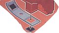 Figure 10. Compliant tape carrying beam leaded chip to bonding site.
 -
 Figure 11. Compliant bonded beam leaded silicon integrated circuit
 -
 Figure 12. Mirror image of the bonded beam leads clearly shown indented in the spent compliant member


Silicon integrated circuit
The two forms of integrated circuits discussed above were the beam leaded integrated circuit composed of attached electroformed gold leads or beams (Figure 5) and the silicon integrated circuit chip (Figure 6). With respect to the beam leaded silicon chip, both compliant and thermocompression bonding can be employed since each have their advantages. At this time,[when?] the most widely used form is the silicon integrated circuit chip, without the beam leads, which therefore requires electrical connections directly to the metallized silicon Chip (Figure 6). If wire connections is the method of choice to form these connections, thermosonic bonding gold wires directly to the silicon chip has been the process most widely used because of its proven reliability as a result of the low bonding parameters of force, temperature, and time needed to form the bond.
References
- ^ Alexander Coucoulas "Bonding With A Compliant Medium". U.S. patent 3,533,155. October 13, 1970. Filed July 6, 1967.
- ^ Coucoulas, A. (1970) “Compliant Bonding” Proceedings 1970 IEEE 20th Electronic Components Conference, pp. 380–89. PDF, PDF2
- .
- .
- ^ Ludwig; David P., Zwickel; Friedich, U.S. patent 4,029,536