Contact resistance
Electrical contact resistance (ECR, or simply contact resistance) is resistance to the flow of electric current caused by incomplete contact of the surfaces through which the current is flowing, and by films or oxide layers on the contacting surfaces. It occurs at
Contact resistance can cause significant voltage drops and heating in circuits with high current. Because contact resistance adds to the intrinsic resistance of the conductors, it can cause significant measurement errors when exact resistance values are needed.
Contact resistance may vary with temperature. It may also vary with time (most often decreasing) in a process known as resistance creep.
Electrical contact resistance is also called interface resistance, transitional resistance, or the correction term. Parasitic resistance is a more general term, of which it is usually assumed that contact resistance is a major component.
William Shockley[1] introduced the idea of a potential drop on an injection electrode to explain the difference between experimental results and the model of gradual channel approximation.
Measurement methods
Because contact resistance is usually comparatively small, it can difficult to measure, and Four-terminal measurement gives better results than a simple two-terminal measurement made with an ohmmeter.
- In a two-terminal measurement (as with a typical ohmmeter), the current used to make the measurement is injected through the measurement leads, which causes a potential drop not just across the contact area to be measured but also across the probe contacts and the leads. That means that the contact resistance of the probes and their leads is inseparable from the resistance of the contact area to be measured, with which they are in series.
- In a four-terminal measurement, the current used to make the measurement is injected using a second, separate pair of leads, so the contact resistance of the measurement probes and their leads is not included in the measurement.
Specific contact resistance can be obtained by multiplying by contact area.

Experimental characterization
For experimental characterization, a distinction must be made between contact resistance evaluation in two-electrode systems (for example, diodes) and three-electrode systems (for example, transistors).
In two-electrode systems, specific contact resistivity is experimentally defined as the slope of the
where J is the current density, or current per area. The units of specific contact resistivity are typically therefore in ohms-square meter, or . When the current is a linear function of the voltage, the device is said to have ohmic contacts. Inductive and capacitive methods could be used in principle to measure an intrinsic impedance without the complication of contact resistance. In practice, direct current methods are more typically used to determine resistance.
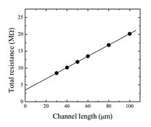
The three electrode systems such as transistors require more complicated methods for the contact resistance approximation. The most common approach is the
where and are contact and channel resistances, respectively, is the channel length/width, is gate insulator capacitance (per unit of area), is carrier mobility, and and are gate-source and drain-source voltages. Therefore, the linear extrapolation of total resistance to the zero channel length provides the contact resistance. The slope of the linear function is related to the channel transconductance and can be used for estimation of the ”contact resistance-free” carrier mobility. The approximations used here (linear potential drop across the channel region, constant contact resistance, …) lead sometimes to the channel dependent contact resistance.[2]
Beside the TLM it was proposed the gated four-probe measurement
In the semiconductor industry, Cross-Bridge Kelvin Resistor(CBKR) structures are the mostly used test structures to characterize metal-semiconductor contacts in the Planar devices of VLSI technology. During the measurement process, force the current (I) between contact 1&2 and measure the potential deference between contacts 3&4. The contact resistance Rk can be then calculated as .[7]
Mechanisms
For given physical and mechanical material properties, parameters that govern the magnitude of electrical contact resistance (ECR) and its variation at an interface relate primarily to
Quantum limit
When a conductor has spatial dimensions close to , where is Fermi wavevector of the conducting material, Ohm's law does not hold anymore. These small devices are called quantum point contacts. Their conductance must be an integer multiple of the value , where is the elementary charge and is
Other forms of contact resistance
Measurements of
Significance
Bad contacts are the cause of failure or poor performance in a wide variety of electrical devices. For example, corroded
See also
References
- ^ Shockley, William (September 1964). "Research and investigation of inverse epitaxial UHF power transistors". Report No. A1-TOR-64-207.
{{cite journal}}: Cite journal requires|journal=(help) - .
- .
- .
- .
- .
- S2CID 111829.
- .
- .
- .
Further reading
- Pitney, Kenneth E. (2014) [1973]. Ney Contact Manual - Electrical Contacts for Low Energy Uses (reprint of 1st ed.). Deringer-Ney, originally JM Ney Co. ] (NB. Free download after registration.)
- Slade, Paul G. (February 12, 2014) [1999]. Electrical Contacts: Principles and Applications. Electrical engineering and electronics. Vol. 105 (2 ed.). )
- ISBN 978-3-540-03875-7. (NB. A rewrite of the earlier "Electric Contacts Handbook".)
- ISBN 978-3-662-42222-9.)
- Huck, Manfred; Walczuk, Eugeniucz; Buresch, Isabell; Weiser, Josef; Borchert, Lothar; Faber, Manfred; Bahrs, Willy; Saeger, Karl E.; Imm, Reinhard; Behrens, Volker; Heber, Jochen; Großmann, Hermann; Streuli, Max; Schuler, Peter; Heinzel, Helmut; Harmsen, Ulf; Györy, Imre; Ganz, Joachim; Horn, Jochen; Kaspar, Franz; Lindmayer, Manfred; Berger, Frank; Baujan, Guenter; Kriechel, Ralph; Wolf, Johann; Schreiner, Günter; Schröther, Gerhard; Maute, Uwe; Linnemann, Hartmut; Thar, Ralph; Möller, Wolfgang; Rieder, Werner; Kaminski, Jan; Popa, Heinz-Erich; Schneider, Karl-Heinz; Bolz, Jakob; Vermij, L.; Mayer, Ursula (2016) [1984]. Vinaricky, Eduard; Schröder, Karl-Heinz; Weiser, Josef; Keil, Albert; Merl, Wilhelm A.; Meyer, Carl-Ludwig (eds.). Elektrische Kontakte, Werkstoffe und Anwendungen: Grundlagen, Technologien, Prüfverfahren (in German) (3 ed.). Berlin / Heidelberg / New York / Tokyo: ISBN 978-3-642-45426-4.


