
Intel 8086
Co-processor Intel 8087, Intel 8089 | | |
| Package(s) |
| |
|---|---|---|
| Socket(s) | ||
| Products, models, variants | ||
| Variant(s) | ||
| History | ||
| Predecessor(s) | Intel 8085 | |
| Successor(s) | 80186 and 80286 (both of which were introduced in early 1982) | |
| Support status | ||
| Unsupported | ||
The 8086[3] (also called iAPX 86)[4] is a 16-bit microprocessor chip designed by Intel between early 1976 and June 8, 1978, when it was released. The Intel 8088, released July 1, 1979,[5] is a slightly modified chip with an external 8-bit data bus (allowing the use of cheaper and fewer supporting ICs),[note 1] and is notable as the processor used in the original IBM PC design.
The 8086 gave rise to the x86 architecture, which eventually became Intel's most successful line of processors. On June 5, 2018, Intel released a limited-edition CPU celebrating the 40th anniversary of the Intel 8086, called the Intel Core i7-8086K.[5]
History
Background
In 1972, Intel launched the
Two years later, Intel launched the
(1978).The first x86 design

The 8086 project started in May 1976 and was originally intended as a temporary substitute for the ambitious and delayed
Whereas the 8086 was a 16-bit microprocessor, it used the same
, so the bus structure was designed to be flexible.The first revision of the instruction set and high level architecture was ready after about three months,[note 5] and as almost no CAD tools were used, four engineers and 12 layout people were simultaneously working on the chip.[note 6] The 8086 took a little more than two years from idea to working product, which was considered rather fast for a complex design in 1976–1978.
The 8086 was sequenced The original chip measured 33 mm² and minimum feature size was 3.2 μm.
The architecture was defined by
Details

Buses and operation
All internal registers, as well as internal and external data buses, are 16 bits wide, which firmly established the "16-bit microprocessor" identity of the 8086. A 20-bit external address bus provides a 1
Hardware modes of 8086
Some of the control pins, which carry essential signals for all external operations, have more than one function depending upon whether the device is operated in min or max mode. The former mode is intended for small single-processor systems, while the latter is for medium or large systems using more than one processor (a kind of multiprocessor mode). Maximum mode is required when using an 8087 or 8089 coprocessor. The voltage on pin 33 (MN/MX) determines the mode. Changing the state of pin 33 changes the function of certain other pins, most of which have to do with how the CPU handles the (local) bus.[note 11] The mode is usually hardwired into the circuit and therefore cannot be changed by software. The workings of these modes are described in terms of timing diagrams in Intel datasheets and manuals. In minimum mode, all control signals are generated by the 8086 itself.
Registers and instruction
| ||||||||||||||||||||||||||||||||||||||||||||||||||||||||||||||||||||||||||||||||||||||||||||||||||||||||||||||||||||||||||||||||||||||||||||||||||||||||||||||||||||||||||||||||||||||||||||||||||||||||||||||||||||||||||||||||||||||||||||||||||||||||||||||||||||||||||||||||||||||||||||||||||||||||||||||||||||||||||||||||||||||||||||||||||||||||||||||||||||||||||||||||||||||||||||||||||||||||||||||||||||||||||||||||||||
The 8086 has eight more-or-less general 16-bit registers (including the stack pointer but excluding the instruction pointer, flag register and segment registers). Four of them, AX, BX, CX, DX, can also be accessed as 8-bit register pairs (see figure) while the other four, SI, DI, BP, SP, are 16-bit only.
Due to a compact encoding inspired by 8-bit processors, most instructions are one-address or two-address operations, which means that the result is stored in one of the operands. At most one of the operands can be in memory, but this memory operand can also be the destination, while the other operand, the source, can be either register or immediate. A single memory location can also often be used as both source and destination which, among other factors, further contributes to a
The degree of generality of most registers is much greater than in the 8080 or 8085. However, 8086 registers were more specialized than in most contemporary
Another factor for this is that the 8086 also introduced some new instructions (not present in the 8080 and 8085) to better support stack-based high-level programming languages such as Pascal and PL/M; some of the more useful instructions are push mem-op, and ret size, supporting the "Pascal calling convention" directly. (Several others, such as push immed and enter, were added in the subsequent 80186, 80286, and 80386 processors.)
A 64 KB (one segment)
The 8086 has 64 K of 8-bit (or alternatively 32 K of 16-bit word)
Flags
The 8086 has a 16-bit
| Bit | 15-12 | 11 | 10 | 9 | 8 | 7 | 6 | 5 | 4 | 3 | 2 | 1 | 0 |
|---|---|---|---|---|---|---|---|---|---|---|---|---|---|
| Flag | OF | DF | IF | TF | SF | ZF | AF | PF | CF |
Segmentation
There are also four 16-bit segment registers (see figure) that allow the 8086 CPU to access one megabyte of memory in an unusual way. Rather than concatenating the segment register with the address register, as in most processors whose address space exceeds their register size, the 8086 shifts the 16-bit segment only four bits left before adding it to the 16-bit offset (16×segment + offset), therefore producing a 20-bit external (or effective or physical) address from the 32-bit segment:offset pair. As a result, each external address can be referred to by 212 = 4096 different segment:offset pairs.
0110 1000 1000 01110000
|
Segment, | 16 bits, shifted 4 bits left (or multiplied by 0x10) |
+ 1011 0100 1010 1001
|
Offset, | 16 bits |
|
||
0111 0011 1101 0001 1001
|
Address, | 20 bits |
Although considered complicated and cumbersome by many programmers, this scheme also has advantages; a small program (less than 64 KB) can be loaded starting at a fixed offset (such as 0000) in its own segment, avoiding the need for relocation, with at most 15 bytes of alignment waste.
Compilers for the 8086 family commonly support two types of
To avoid the need to specify near and far on numerous pointers, data structures, and functions, compilers also support "memory models" which specify default pointer sizes. The tiny (max 64K), small (max 128K), compact (data > 64K), medium (code > 64K), large (code,data > 64K), and huge (individual arrays > 64K) models cover practical combinations of near, far, and huge pointers for code and data. The tiny model means that code and data are shared in a single segment, just as in most 8-bit based processors, and can be used to build .com files for instance. Precompiled libraries often come in several versions compiled for different memory models.
According to Morse et al.,.[10] the designers actually contemplated using an 8-bit shift (instead of 4-bit), in order to create a 16 MB physical address space. However, as this would have forced segments to begin on 256-byte boundaries, and 1 MB was considered very large for a microprocessor around 1976, the idea was dismissed. Also, there were not enough pins available on a low cost 40-pin package for the additional four address bus pins.
In principle, the address space of the x86 series could have been extended in later processors by increasing the shift value, as long as applications obtained their segments from the operating system and did not make assumptions about the equivalence of different segment:offset pairs.[note 12] In practice the use of "huge" pointers and similar mechanisms was widespread and the flat 32-bit addressing made possible with the 32-bit offset registers in the 80386 eventually extended the limited addressing range in a more general way.
The instruction stream is fetched from memory as words and is addressed internally by the processor to the byte level as necessary. An instruction stream queuing mechanism allows up to 6 bytes of the instruction stream to be queued while waiting for decoding and execution. The queue acts as a First-In-First-Out (FIFO) buffer, from which the Execution Unit (EU) extracts instruction bytes as required. Whenever there is space for at least two bytes in the queue, the BIU will attempt a word fetch memory cycle. If the queue is empty (following a branch instruction, for example), the first byte into the queue immediately becomes available to the EU.[11]
Porting older software
Small programs could ignore the segmentation and just use plain 16-bit addressing. This allows
Example code
The following 8086
0000 0000 55 0001 89 E5 0003 56 0004 57 0005 8B 75 06 0008 8B 7D 04 000B FC 000C AC 000D 3C 41 000F 7C 06 0011 3C 5A 0013 7F 02 0015 04 20 0017 AA 0018 08 C0 001A 75 F0 001C 5F 001D 5E 001E 5D 001F C3 001F |
; _strtolower:
; Copy a null-terminated ASCII string, converting
; all alphabetic characters to lower case.
; ES=DS
; Entry stack parameters
;      [SP+4] = src, Address of source string
;      [SP+2] = dst, Address of target string
;      [SP+0] = Return address
;
_strtolower proc
            push    bp             ;Set up the call frame
            mov     bp,sp
            push    si
            push    di
            mov     si,[bp+6]       ;Set SI = src (+2 due to push bp)
            mov     di,[bp+4]       ;Set DI = dst
            cld                     ;string direction ascending

loop:       lodsb                   ;Load AL from [si], inc si
            cmp     al,'A'          ;If AL < 'A',
            jl      copy            ; Skip conversion
            cmp     al,'Z'          ;If AL > 'Z',
            jg      copy            ; Skip conversion
            add     al,'a'-'A'      ;Convert AL to lowercase
copy:       stosb                   ;Store AL to [di], inc di
            or      al,al           ;If AL <> 0,
            jne     loop            ; Repeat the loop

done:       pop     di              ; restore di and si
            pop     si
            pop     bp              ;Restore the prev call frame
            ret                     ;Return to caller
            end     proc
|
The example code uses the BP (base pointer) register to establish a
Performance

Although partly shadowed by other design choices in this particular chip, the
| instruction | register-register | register immediate | register-memory | memory-register | memory-immediate |
|---|---|---|---|---|---|
| mov | 2 | 4 | 8+EA | 9+EA | 10+EA |
| ALU | 3 | 4 | 9+EA, | 16+EA, | 17+EA |
| jump | register ≥ 11 ; label ≥ 15 ; condition,label ≥ 16 | ||||
| integer multiply | 70~160 (depending on operand data as well as size) including any EA | ||||
| integer divide | 80~190 (depending on operand data as well as size) including any EA | ||||
- EA = time to compute effective address, ranging from 5 to 12 cycles.
- Timings are best case, depending on prefetch status, instruction alignment, and other factors.
As can be seen from these tables, operations on registers and immediates were fast (between 2 and 4 cycles), while memory-operand instructions and jumps were quite slow; jumps took more cycles than on the simple 8080 and 8085, and the 8088 (used in the IBM PC) was additionally hampered by its narrower bus. The reasons why most memory related instructions were slow were threefold:
- Loosely coupled fetch and execution units are efficient for instruction prefetch, but not for jumps and random data access (without special measures).
- No dedicated address calculation adder was afforded; the microcode routines had to use the main ALU for this (although there was a dedicated segment + offset adder).
- The address and data buses were multiplexed, forcing a slightly longer (33~50%) bus cycle than in typical contemporary 8-bit processors.[dubious ]
However, memory access performance was drastically enhanced with Intel's next generation of 8086 family CPUs. The 80186 and 80286 both had dedicated address calculation hardware, saving many cycles, and the 80286 also had separate (non-multiplexed) address and data buses.
Floating point
The 8086/8088 could be connected to a mathematical coprocessor to add hardware/microcode-based
Chip versions
The clock frequency was originally limited to 5 MHz,
The 80C86, the CMOS version of the 8086, was used in the GRiDPad, Toshiba T1200, HP 110, and finally the 1998–1999 Lunar Prospector.
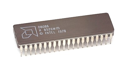
For the packaging, the Intel 8086 was available both in ceramic and plastic DIP packages.
-
 A ceramic D8086 variant
 -
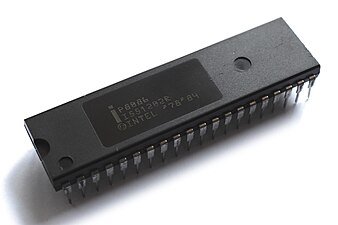 A plastic P8086 variant


List of Intel 8086
| Model number | Frequency | Technology | Temperature range | Package | Date of release | Price (USD)[list2 1] |
|---|---|---|---|---|---|---|
| 8086 | 5 MHz[13] | HMOS | 0 °C to 70 °C[14] | June 8, 1978[15] | $86.65[16] | |
| 8086-1 | 10 MHz | HMOS II | Commercial | |||
| 8086-2 | 8 MHz[13] | HMOS II | Commercial | January/February 1980[17] | $200[17][18] | |
| 8086-4 | 4 MHz[13] | HMOS | Commercial | $72.50[list2 2][19] | ||
| I8086 | 5 MHz | HMOS | Industrial −40 °C to +85 °C[14] | May/June 1980[14] | $173.25[14] | |
| M8086 | 5 MHz | HMOS | Military grade −55 °C to +125 °C[20] | |||
| 80C86[21] | CMOS | 44 Pin PLCC[list2 3][22] |
Derivatives and clones
Compatible—and, in many cases, enhanced—versions were manufactured by
The electronics industry of the Soviet Union was able to replicate the 8086 through both industrial espionage and reverse engineering[citation needed]. The resulting chip, K1810VM86, was binary and pin-compatible with the 8086.
i8086 and i8088 were respectively the cores of the Soviet-made PC-compatible EC1831 and EC1832 desktops. (EC1831 is the EC identification of IZOT 1036C and EC1832 is the EC identification of IZOT 1037C, developed and manufactured in Bulgaria. EC stands for Единая Система.) However, the EC1831 computer (IZOT 1036C) had significant hardware differences from the IBM PC prototype. The EC1831 was the first PC-compatible computer with dynamic bus sizing (US Pat. No 4,831,514). Later some of the EC1831 principles were adopted in PS/2 (US Pat. No 5,548,786) and some other machines (UK Patent Application, Publication No. GB-A-2211325, Published June 28, 1989).
-
 Soviet clone K1810VM86
 -
 QFP-56
 -
 NEC μPD8086D-2 (8 MHz) from the year 1984, week 19 JAPAN (clone of Intel D8086-2)
 -
 The AMD D8086


Support chips
- Intel 8237: direct memory access (DMA) controller
- Intel 8251: universal synchronous/asynchronous receiver/transmitter at 19.2 kbit/s
- Intel 8253: programmable interval timer, 3x 16-bit max 10 MHz
- Intel 8255: programmable peripheral interface, 3x 8-bit I/O pins used for printer connection etc.
- Intel 8259: programmable interrupt controller
- Intel 8279: keyboard/display controller, scans a keyboard matrix and display matrix like 7-seg
- Intel 8282/8283: 8-bit latch
- Intel 8284: clock generator
- Intel 8286/8287: bidirectional 8-bit driver. In 1980 both Intel I8286/I8287 (industrial grade) version were available for US$16.25 in quantities of 100.[14]
- Intel 8288: bus controller
- Intel 8289: bus arbiter
- NEC µPD765 or Intel 8272A: floppy controller[24]
Microcomputers using the 8086
- The Intel Multibus-compatible single-board computer ISBC 86/12 was announced in 1978.[25]
- The Xerox NoteTaker was one of the earliest portable computer designs in 1978 and used three 8086 chips (as CPU, graphics processor, and I/O processor), but never entered commercial production.
- Seattle Computer Products shipped S-100 bus based 8086 systems (SCP200B) as early as November 1979.
- The Norwegian Mycron 2000, introduced in 1980.
- One of the most influential microcomputers of all, the IBM PC, used the Intel 8088, a version of the 8086 with an 8-bit data bus(as mentioned above).
- The first IBM PC XTand could switch the CPU down to the lower speed (which also switched in a memory bus buffer to simulate the 8088's slower access) to avoid software timing issues.
- An 8 MHz 8086-2 was used in the IBM PC AT, but different in the design details, and physically incompatible), and all system peripherals including the onboard video system also enjoy 16-bit data transfers. The later Olivetti M24SP featured an 8086-2 running at the full maximum 10 MHz.
- The were built with an 8 MHz 8086.
- The PC1640, PC2086, PC3086 and PC5086 all used 8086 CPUs at 8 MHz.
- The NEC PC-9801.
- The Tandy 1000 SL-series and RL machines used 9.47 MHz 8086 CPUs.
- The IBM Displaywriter word processing machine[26] and the Wang Professional Computer, manufactured by Wang Laboratories, also used the 8086.
- NASA used original 8086 CPUs on equipment for ground-based maintenance of the Space Shuttle Discovery until the end of the space shuttle program in 2011. This decision was made to prevent software regression that might result from upgrading or from switching to imperfect clones.[27]
- KAMAN Process and Area Radiation Monitors[28]
- The Tektronix 4170 ran CP/M-86 and used an 8086 4170 Local Graphics Processing Unit Instruction Manual (PDF)
See also
- Transistor count
- iAPX, for the iAPX name
Notes
- ^ Fewer TTL buffers, latches, multiplexers (although the amount of TTL logic was not drastically reduced). It also permits the use of cheap 8080-family ICs, where the 8254 CTC, 8255 PIO, and 8259 PIC were used in the IBM PC design. In addition, it makes PCB layout simpler and boards cheaper, as well as demanding fewer (1- or 4-bit wide) DRAM chips.
- ^ using enhancement load PMOS logic (requiring 14 V, achieving TTL compatibility by having VCC at +5 V and VDD at −9 V).
- ^ Using non-saturated enhancement-load NMOS logic (demanding a higher gate voltage for the load-transistor gates).
- ^ Made possible with depletion-load nMOS logic (the 8085 was later made using HMOS processing, just like the 8086).
- ^ Rev.0 of the instruction set and architecture was ready in about three months, according to Morse.
- digitizer(according to Jenny Hernandez, member of the 8086 design team, in a statement made on Intel's webpage for its 25th birthday).
- ^ 8086 used less microcode than many competitors' designs, such as the MC68000 and others
- ^ Fast static RAMs in MOS technology (as fast as bipolar RAMs) was an important product for Intel during this period.
- HMOS.
- ^ Other members of the design team were Peter A.Stoll and Jenny Hernandez.
- ^ The IBM PC and PC/XT use an Intel 8088 running in maximum mode, which allows the CPU to work with an optional 8087 coprocessor installed in the math coprocessor socket on the PC or PC/XT mainboard. (The PC and PC/XT may require maximum mode for other reasons, such as perhaps to support the DMA controller.)
- ^ Some 80186 clones did change the shift value, but were never commonly used in desktop computers.
- color burstfrequency)
References
- ^ "The Life Cycle of a CPU". www.cpushack.com.
- ^ Lewnes, Ann, "The Intel386 Architecture Here to Stay", Intel Corporation, Microcomputer Solutions, July/August 1989, page 2
- ^ "Microprocessor Hall of Fame". Intel. Archived from the original on 2007-07-06. Retrieved 2007-08-11.
- ^ iAPX 286 Programmer's Reference (PDF). Intel. 1983. p. 1-1.
- ^ a b "Happy Birthday, 8086: Limited-Edition 8th Gen Intel Core i7-8086K Delivers Top Gaming Experience". Intel.
- ^ "8080 family". CPU World.
- 8080at the assembly-language level. […]
- ISBN 0-07-023253-9. — Illustration of use of "random" describing CPU control logic
- OCLC 11091251.
- S2CID 206445851.
- ^ "8086 16-BIT HMOS Processor datasheet" (PDF). Intel. Retrieved 26 November 2021.
- Microsoft Macro Assembler 5.0 Reference Manual. Microsoft Corporation. 1987.
Timings and encodings in this manual are used with permission of Intel and come from the following publications: Intel Corporation. iAPX 86, 88, 186 and 188 User's Manual, Programmer's Reference, Santa Clara, Calif. 1986.
(Similarly for iAPX 286, 80386, 80387.) - ^ OCLC 65699372.
- ^ OCLC 803251993.
- ^ "Intel® Microprocessor Quick Reference Guide - Year". www.intel.com.
- OCLC 10331599.
- ^ a b Intel Corporation (January–February 1980). "New Products: Faster 8086 provides 60% more performance". Intel Preview: 22.
- ^ Intel Corporation (May–June 1980). "New 8086 family products boost processor performance by 50 percent". Intel Preview (Special Issue: 16-Bit Solutions): 17.
- ^ Intel Corporation (May–June 1979). "Microcomputer Components: New price reductions and production improvements make the popular 8086 microprocessor even more attractive". Intel Preview: 11.
- OCLC 8459750.
- ^ Intel Corporation, "NewsBit: Intel Licenses Oki on CMOS Version of Several Products", Solutions, July/August 1984, Page 1.
- ^ Ashborn, Jim; "Advanced Packaging: A Little Goes A Long Way", Intel Corporation, Solutions, January/February 1986, Page 2
- ^ Intel Corporation, "NewsBits: Second Source News", Solutions, January/February 1985, Page 1
- ^ "The floppy controller evolution | OS/2 Museum". 2011-05-26. Retrieved 2016-05-12.
In the original IBM PC (1981) and PC/XT (1983), the FDC was physically located on a separate diskette adapter card. The FDC itself was a NEC µPD765A or a compatible part, such as the Intel 8272A.
- ISSN 0010-4841.
- ISSN 0199-6649.
the IBM Displaywriter is noticeably more expensive than other industrial micros that use the 8086.
- ^ "For Old Parts, NASA Boldly Goes ... on eBay". New York Times. May 12, 2002.
- ^ Kaman Tech. Manual
External links
- Intel datasheets
- List of 8086 CPUs and their clones at CPUworld.com
- 8086 Pinouts
- Maximum Mode Interface Archived from the original on July 21, 2011. Retrieved July 10, 2022.
- The 8086 User's manual October 1979 INTEL Corporation (PDF document)
- 8086 program codes using emu8086 (Version 4.08) Emulator
- Jenner, Andrew (September 2020). "8086 microcode disassembled". Reenigne blog.
- Shirriff, Ken (June 2020). "A look at the die of the 8086 processor".
- — (June 2020). "Die shrink: How Intel scaled down the 8086 processor".
- — (July 2020). "The Intel 8086 processor's registers: from chip to transistors".
- — (August 2020). "Reverse-engineering the adder inside the Intel 8086".
- — (August 2020). "Reverse-engineering the 8086's Arithmetic/Logic Unit from die photos".
- — (November 2022). "The unusual bootstrap drivers inside the 8086 microprocessor chip".
- — (November 2022). "A bug fix in the 8086 microprocessor, revealed in the die's silicon".
- — (December 2022). "How the 8086 processor's microcode engine works".
- — (January 2023). "Inside the 8086 processor's instruction prefetch circuitry".
- — (January 2023). "The 8086 processor's microcode pipeline from die analysis".
- — (January 2023). "Counting the transistors in the 8086 processor: it's harder than you might think".
- — (January 2023). "Reverse-engineering the conditional jump circuitry in the 8086 processor".
- — (January 2023). "Reverse-engineering the Intel 8086 processor's HALT circuits".
- — (January 2023). "Understanding the x86's Decimal Adjust after Addition (DAA) instruction".
- — (February 2023). "Silicon reverse-engineering: the Intel 8086 processor's flag circuitry".
- — (February 2023). "Reverse-engineering the interrupt circuitry in the Intel 8086 processor".
- — (February 2023). "Reverse-engineering the ModR/M addressing microcode in the Intel 8086 processor".
- — (March 2023). "How the 8086 processor determines the length of an instruction".