Molecular-beam epitaxy

Molecular-beam epitaxy (MBE) is an
History
Original ideas of MBE process were first established by K. G. Günther.[3] Films he deposited were not epitaxial, but were deposited on glass substrates. With the development of vacuum technology, MBE process was demonstrated by John Davey and Titus Pankey who succeeded in growing GaAs epitaxial films on single crystal GaAs substrates using Günther's method. Major subsequent development of MBE films was enabled by J.R. Arthur's investigations of kinetic behavior of growth mechanisms and Alfred Y. Cho's in situ observation of MBE process using reflection high-energy electron diffraction (RHEED) in the late 1960s.[4][5][6]
Method
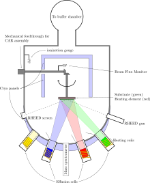
Molecular-beam epitaxy takes place in

In solid source MBE, elements such as
During operation,
In systems where the substrate needs to be cooled, the ultra-high vacuum environment within the growth chamber is maintained by a system of
Molecular-beam epitaxy (MBE) is also used for the deposition of some types of organic semiconductors. In this case, molecules, rather than atoms, are evaporated and deposited onto the wafer. Other variations include gas-source MBE, which resembles chemical vapor deposition.

MBE systems can also be modified according to need. Oxygen sources, for example, can be incorporated for depositing oxide materials for advanced electronic, magnetic and optical applications, as well as for fundamental research. Here, a molecular beam of an oxidant is used to achieve the desired oxidation state of a multicomponent oxide.
Quantum nanostructures
One of the most accomplished achievements of molecular-beam epitaxy is the nano-structures that permitted the formation of atomically flat and abrupt hetero-interfaces. Such structures have played an unprecedented role in expanding the knowledge of physics and electronics.
Asaro–Tiller–Grinfeld instability
The Asaro–Tiller–Grinfeld (ATG) instability, also known as the Grinfeld instability, is an elastic instability often encountered during molecular-beam epitaxy. If there is a mismatch between the lattice sizes of the growing film and the supporting crystal, elastic energy will be accumulated in the growing film. At some critical height, the free energy of the film can be lowered if the film breaks into isolated islands, where the tension can be relaxed laterally. The critical height depends on the Young's modulus, mismatch size, and surface tension.
Some applications for this instability have been researched, such as the self-assembly of quantum dots. This community uses the name of Stranski–Krastanov growth for ATG.
See also
- Pulsed laser deposition
- Metalorganic vapour phase epitaxy
- Colin P. Flynn
- Arthur Gossard
- High-electron-mobility transistor (HEMT)
- Heterojunction bipolar transistor
- Herbert Kroemer
- Quantum cascade laser
- Solar cell
- Ben G. Streetman
- Wetting layer
- Thermal Laser Epitaxy
Notes
- S2CID 205442147.
- ^ "Alfred Y. Cho". National Inventors Hall of Fame. Retrieved 17 August 2019.
- S2CID 97543040.
- .
- .
- ISBN 978-1-4614-9286-3.
- .
- S2CID 29612904.
- .
- PMID 26618638.
- ^ Mayer, B., et al. "Long-term mutual phase locking of picosecond pulse pairs generated by a semiconductor nanowire laser". Nature Communications 8 (2017): 15521.
References
- Jaeger, Richard C. (2002). "Film Deposition". Introduction to Microelectronic Fabrication (2nd ed.). Upper Saddle River: Prentice Hall. ISBN 978-0-201-44494-0.
- McCray, W. P. (2007). "MBE Deserves a Place in the History Books". S2CID 205442147.
- Shchukin, Vitaliy A.; Dieter Bimberg (1999). "Spontaneous ordering of nanostructures on crystal surfaces". .
- Stangl, J.; V. Holý; G. Bauer (2004). "Structural properties of self-organized semiconductor nanostructures" (PDF). .
Further reading
- Frigeri, P.; Seravalli, L.; Trevisi, G.; Franchi, S. (2011). "3.12: Molecular Beam Epitaxy: An Overview". In Pallab Bhattacharya; Roberto Fornari; Hiroshi Kamimura (eds.). Comprehensive Semiconductor Science and Technology. Vol. 3. Amsterdam: Elsevier. pp. 480–522. ISBN 978-0-444-53153-7.
