
Organic electronics

Organic electronics is a field of materials science concerning the design, synthesis, characterization, and application of organic molecules or polymers that show desirable electronic properties such as conductivity. Unlike conventional inorganic conductors and semiconductors, organic electronic materials are constructed from organic (carbon-based) molecules or polymers using synthetic strategies developed in the context of organic chemistry and polymer chemistry.
One of the promised benefits of organic electronics is their potential low cost compared to traditional electronics.
History
- Electrically conductive polymers
Traditional conductive materials are
In 1862
J.E. Lilienfeld[6] first proposed the field-effect transistor in 1930, but the first OFET was not reported until 1987, when Koezuka et al. constructed one using Polythiophene[7] which shows extremely high conductivity. Other conductive polymers have been shown to act as semiconductors, and newly synthesized and characterized compounds are reported weekly in prominent research journals. Many review articles exist documenting the development of these materials.[8][9][10][11][12]
In 1987, the first organic
- Electrically conductive charge transfer salts
In the 1950s, organic molecules were shown to exhibit electrical conductivity. Specifically, the organic compound
- Light and electrical conductivity
André Bernanose[15][16] was the first person to observe electroluminescence in organic materials. Ching W. Tang and Steven Van Slyke,[17] reported fabrication of the first practical OLED device in 1987. The OLED device incorporated a double-layer structure motif composed of copper phthalocyanine and a derivative of perylenetetracarboxylic dianhydride.[18]
In 1990, a
Conductive organic materials
Organic conductive materials can be grouped into two main classes: polymers and conductive molecular solids and salts. Polycyclic aromatic compounds such as pentacene and rubrene often form semiconducting materials when partially oxidized.
Organic light-emitting diode
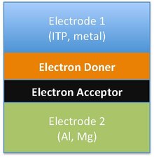
An OLED (organic light-emitting diode) consists of a thin film of organic material that emits light under stimulation by an electric current. A typical OLED consists of an anode, a cathode, OLED organic material and a conductive layer.[23]


OLED organic
Organic field-effect transistor

An organic field-effect transistor (OFET) is a field-effect transistor utilizing organic molecules or polymers as the active semiconducting layer. A field-effect transistor (
As for OLEDs, some OFETs are molecular and some are polymer-based system.
Organic electronic devices

Organic solar cells could cut the cost of solar power compared with conventional solar-cell manufacturing.[27] Silicon thin-film solar cells on flexible substrates allow a significant cost reduction of large-area photovoltaics for several reasons:[28]
- The so-called 'glass sheets.
- Transport and installation of lightweight flexible solar cells also saves cost as compared to cells on glass.
Inexpensive polymeric substrates like polyethylene terephthalate (PET) or polycarbonate (PC) have the potential for further cost reduction in photovoltaics. Protomorphous solar cells prove to be a promising concept for efficient and low-cost photovoltaics on cheap and flexible substrates for large-area production as well as small and mobile applications.[28]
One advantage of printed electronics is that different electrical and electronic components can be printed on top of each other, saving space and increasing reliability and sometimes they are all transparent. One ink must not damage another, and low temperature annealing is vital if low-cost flexible materials such as paper and plastic film are to be used. There is much sophisticated engineering and chemistry involved here, with iTi, Pixdro, Asahi Kasei, Merck & Co.|Merck, BASF, HC Starck, Hitachi Chemical and Frontier Carbon Corporation among the leaders.[29]
Fabrication methods
Small molecule semiconductors are often
Organic solar cells
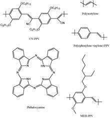
Organic semiconductor diodes convert light into electricity. Figure to the right shows five commonly used organic photovoltaic materials. Electrons in these organic molecules can be delocalized in a delocalized π
The difference in the

Organic field-effect transistors
An organic field-effect transistor is a three terminal device (source, drain and gate). The charge carriers move between source and drain, and the gate serves to control the path's conductivity. There are mainly two types of organic field-effect transistor, based on the semiconducting layer's charge transport, namely p-type (such as dinaphtho[2,3-b:2′,3′-f]thieno[3,2-b]thiophene, DNTT),[36] and n-type (such phenyl C61 butyric acid methyl ester, PCBM).[37] Certain organic semiconductors can also present both p-type and n-type (i.e., ambipolar) characteristics.[38]
Such technology allows for the fabrication of large-area, flexible, low-cost electronics.[39] One of the main advantages is that being mainly a low temperature process compared to CMOS, different type of materials can be utilized. This makes them in turn great candidates for sensing.[40]
Features
Conductive polymers are lighter, more flexible, and less expensive than inorganic conductors. This makes them a desirable alternative in many applications. It also creates the possibility of new applications that would be impossible using copper or silicon.
Organic electronics not only includes
New applications include
See also
- Annealing
- Bioplastic
- Carbon nanotube
- Circuit deposition
- Conductive ink
- Flexible display
- Laminar
- Melanin
- Organic field-effect transistor (OFET)
- Organic semiconductor
- Organic light-emitting diode
- Photodetector
- Printed electronics
- Radio frequency identification
- Radio tag
- Schön scandal
- Spin coating
References
- ISBN 9783527312641.
- ISBN 9783527640218electronic bk.
- ISBN 978-3-527-32611-2
- .
- ^ "The Nobel Prize in Chemistry 2000". Nobelprize.org. Nobel Media.
- ^ CA 272437, Lilienfeld, Julius Edgar, "Electric current control mechanism", published 1927-07-19
- .
- PMID 27877287.
- PMID 27877286.
- .
- .
- PMID 20396828.
- .
- ISSN 0002-7863.
- .
- .
- ^ doi:10.1063/1.98799.
- .
- S2CID 43158308.
- S2CID 4393960.
- ISBN 978-0-309-30591-4.
- .
- ISBN 978-1466515185.
- .
- .
- S2CID 43158308.
- ^ Bullis, Kevin (17 October 2008). "Mass Production of Plastic Solar Cells". Technology Review.
- ^ a b Koch, Christian (2002) Niedertemperaturabscheidung von Dünnschicht-Silicium für Solarzellen auf Kunststofffolien, Doctoral Thesis, ipe.uni-stuttgart.de
- ^ Raghu Das, IDTechEx (25 September 2008). "Printed electronics, is it a niche? – 25 September 2008". Electronics Weekly. Retrieved 14 February 2010.
- ^ プラスチックフィルム上の有機TFT駆動有機ELディスプレイで世界初のフルカラー表示を実現. sony.co.jp (in Japanese)
- ^ Flexible, full-color OLED display. pinktentacle.com (24 June 2007).
- .
- ISBN 978-1860941610.
- .
- S2CID 43074502.
- .
- S2CID 205235378.
- S2CID 6042903.
- S2CID 26645918.
- ISSN 0925-4005.
Further reading
- Grasser, Tibor., Meller, Gregor. Baldo, Marc. (Eds.) (2010) Organic electronics Springer, Heidelberg. ISBN 978-3-642-04537-0(Print) 978-3-642-04538-7 (Online)
- Baracus, B. A.; Weiss, D. E. (1963). "Electronic Conduction in Polymers. II. The Electrochemical Reduction of Polypyrrole at Controlled Potential". Aust. J. Chem. 16 (6): 1076–1089. .
- Bolto, B. A.; McNeill, R.; Weiss, D. E. (1963). "Electronic Conduction in Polymers. III. Electronic Properties of Polypyrrole". Aust. J. Chem. 16 (6): 1090–1103. .
- Hush, Noel S. (2003). "An Overview of the First Half-Century of Molecular Electronics". Ann. N.Y. Acad. Sci. 1006 (1): 1–20. S2CID 24968273.
- Electronic Processes in Organic Crystals and Polymers, 2 ed. by Martin Pope and Charles E. Swenberg, Oxford University Press (1999), ISBN 0-19-512963-6
- Handbook of Organic Electronics and Photonics (3-Volume Set) by Hari Singh Nalwa, American Scientific Publishers. (2008), ISBN 1-58883-095-0
External links
 Media related to Organic electronics at Wikimedia Commons
- orgworld – Organic Semiconductor World homepage.
| Authority control databases: National |
|---|