Tunnel diode
Quantum tunneling | |
| Invented | Leo Esaki |
|---|---|
| First production | Sony |
| Pin configuration | anode and cathode |
| Electronic symbol | |
 | |

A tunnel diode or Esaki diode is a type of
Tunnel diodes have a heavily
Uses
The

Due to their low output power, tunnel diodes are not widely used: Their
Another type of tunnel diode is a
Forward bias operation
Under normal
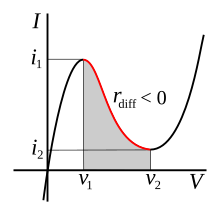
at first tunnel through the very narrow P-N junction barrier and fill electron states in the conduction band on the N-side which become aligned with empty valence band hole states on the P-side of the P-N junction. As voltage increases further, these states become increasingly misaligned, and the current drops. This is called negative differential resistance because current decreases with increasing voltage. As voltage increases beyond a fixed transition point, the diode begins to operate as a normal diode, where electrons travel by conduction across the P-N junction, and no longer by tunneling through the P–N junction barrier. The most important operating region for a tunnel diode is the "negative resistance" region. Its graph is different from normal P-N junction diode.Reverse bias operation

When used in the reverse direction, tunnel diodes are called back diodes (or backward diodes) and can act as fast
Technical comparisons

In a conventional semiconductor diode, conduction takes place while the P-N junction is forward biased and blocks current flow when the junction is reverse biased. This occurs up to a point known as the "reverse breakdown voltage" at which point conduction begins (often accompanied by destruction of the device). In the tunnel diode, the dopant concentrations in the P and N layers are increased to a level such that the reverse breakdown voltage becomes zero and the diode conducts in the reverse direction. However, when forward-biased, an effect occurs called
Applications
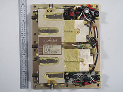
The tunnel diode showed great promise as an oscillator and high-frequency threshold (trigger) device since it operated at frequencies far greater than the tetrode could: well into the microwave bands. Applications of tunnel diodes included local oscillators for UHF television tuners, trigger circuits in oscilloscopes, high-speed counter circuits, and very fast-rise time pulse generator circuits. In 1977, the Intelsat V satellite receiver used a microstrip tunnel diode amplifier (TDA) front-end in the 14–15.5 GHz frequency band. Such amplifiers were considered state-of-the-art, with better performance at high frequencies than any transistor-based front end.[11] The tunnel diode can also be used as a low-noise microwave amplifier.[7]: 13–64 Since its discovery, more conventional semiconductor devices have surpassed its performance using conventional oscillator techniques. For many purposes, a three-terminal device, such as a field-effect transistor, is more flexible than a device with only two terminals. Practical tunnel diodes operate at a few milliamperes and a few tenths of a volt, making them low-power devices.[12] The Gunn diode has similar high frequency capability and can handle more power.
Tunnel diodes are also more resistant to ionizing radiation than other diodes.[citation needed] This makes them well suited to higher radiation environments such as those found in space.
Longevity
Tunnel diodes are susceptible to damage by overheating, and thus special care is needed when soldering them.
Tunnel diodes are notable for their longevity, with devices made in the 1960s still functioning. Writing in Nature, Esaki and coauthors state that semiconductor devices in general are extremely stable, and suggest that their shelf life should be "infinite" if kept at room temperature. They go on to report that a small-scale test of 50 year-old devices revealed a "gratifying confirmation of the diode's longevity". As noticed on some samples of Esaki diodes, the gold-plated iron pins can in fact corrode and short out to the case. This can usually be diagnosed and treated with simple peroxide / vinegar technique normally used for repairing phone PCBs and the diode inside normally still works.[13]
Surplus Russian components are also reliable and often can be purchased for a few pence, despite original cost being in the £30–50 range. The units typically sold are GaAs based and have a Ipk⁄Iv ratio of 5:1 at around 1–20 mA Ipk, and so should be protected against overcurrent.[14]
See also
References
- .
- ^ "Chapter 9: The Model 2T7 Transistor". www.sony.net. Sony History. Sony Global. Retrieved 4 April 2018.
- ^ "The Nobel Prize in Physics 1973: Award ceremony speech". NobelPrize.org. Retrieved 2023-12-17.
- ISBN 0-19-516343-5.
- ^ ソニー半導体の歴史 (in Japanese). Archived from the original on 2 February 2009.
- ^ Rostky, George. "Tunnel diodes: the transistor killers". EE Times. Archived from the original on 7 January 2010. Retrieved 2 October 2009.
- ^ ISBN 0-07-020980-4.
- ISSN 0003-6951. Archived from the original(PDF) on 23 September 2015. Retrieved 26 December 2012.
- OSU College of Engineering.
- ^ "The MIM diode: Another challenger for the electronics crown". SciTechStory. 19 November 2010. Archived from the original on 24 December 2016. Retrieved 4 January 2017.
- ISSN 0095-9669.
- ISBN 0-408-00168-2.
- PMID 20203587.
- ^ "Russian tunnel diodes". w140.com. TekWiki. Retrieved 13 November 2023.
