UltraRAM
This article may be too technical for most readers to understand. (April 2022) |

| Computer memory and Computer data storage types |
|---|
| Volatile |
| Non-volatile |
UltraRAM is a brand name and a storage device technology that is under development. The Physics and Engineering department of Lancaster University in collaboration with Department of Physics at Warwick published a paper[1] in the journal of advanced electronic materials suggesting an improvement in non volatile memory technology. It has been described as a memory storage technology that "combines the non-volatility of a data storage memory, like flash, with the speed, energy-efficiency, and endurance of a working memory, like DRAM" which means it could retain data like a hard drive.[2] While the Lancaster team performed some basic experiments to demonstrate the principles in action, UltraRAM remains mostly theoretical at the moment.[3] The Lancaster University researchers say that further work is ongoing to improve quality, fine-tune the fabrication process, and implement and scale UltraRAM devices.[4]
History
In 2023 Quinas company formed to further develop Ultraram.[5]
Memory Concept
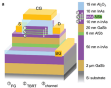
ULTRARAM is a charge-based memory where the logic state is determined by the presence or absence of electrons in an FG (Front Gate). The FG is electrically isolated from the control gate (CG) by Al2O3 dielectric, and from the underlying channel by the InAs/AlSb TBRT heterostructure. The presence of electrons in the FG (defining a logic 0 state) depletes carriers in the underlying n-type InAs channel, reducing its conductance. Thus, the charge state of the FG and, therefore, the logic state of the memory, is read nondestructively by measuring the current through the channel when a voltage is applied between the source (S) and drain (D) contacts. The final component of the memory is the InAs back-gate (BG), which allows voltages to be applied vertically across the gate stack for various operations.
The novelty underpinning the memory is the TBRT (Triple Barrier
Operations

A charged FG is defined as logic '0', and the absence of charge as logic '1'. Program and erase cycles, to charge and discharge the FG respectively, use voltage pulses of ≤±2.55 V on the CG.
InAs channel transistors with submicrometer feature sizes and a subthreshold swing of <100 mV/dec have previously been demonstrated.[6] Consequently, due to the threshold voltage window of 350 mV in the devices designed by the Lancaster team, one can expect the 0/1 current contrast of ULTRARAM to improve to three decades with the implementation of a normally-off channel. Such an improvement of the 0/1 contrast through careful modification of the channel will allow memory arrays to be built with a novel high-density RAM architecture.[1]
Significance
The ULTRARAM on silicon devices actually outperform previous incarnations of the technology on
Accolades
On August 11, 2023, it won the "Most Innovative Flash Memory Startup" award at the 17th Flash Memory Summit (FMS 2023). [7]
See also
References
- ^ S2CID 248070399.
- ^ a b "Mass production of revolutionary computer memory moves closer with ULTRARAM on silicon wafers for the first time". ScienceDaily. Retrieved 2022-04-08.
- ^ "'UltraRAM' breakthrough could merge storage and RAM into one component". PCWorld. Retrieved 2022-04-08.
- ^ Mark Tyson (2022-01-10). "UltraRAM Breakthrough Brings New Memory and Storage Tech to Silicon". Tom's Hardware. Retrieved 2022-04-08.
- ^ Mark Tyson (2023-09-26). "UltraRAM Demos Prototype Chip, Secures Funding to Validate Commercial Potential". Tom's Hardware. Retrieved 2023-09-26.
- S2CID 10847457.
- ^ "Flash Memory Summit Announces 2023 Best of Show Award Winners". kalkinemedia.com. 2023-08-12. Retrieved 2023-09-28.
External links
- Nasser, Hussein (19 Jan 2022). "Is ULTRARAM a game changer?". YouTube.
- Promotion video: https://www.youtube.com/watch?v=iz-sYyfojw4
