Walter Houser Brattain
Walter Houser Brattain | |
|---|---|
Bell Laboratories | |
| Doctoral advisor | John Torrence Tate Sr. |
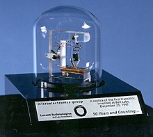
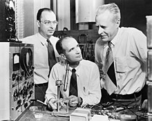
Walter Houser Brattain (/ˈbrætən/; February 10, 1902 – October 13, 1987) was an American physicist at Bell Labs who, along with fellow scientists John Bardeen and William Shockley, invented the point-contact transistor in December 1947.[1] They shared the 1956 Nobel Prize in Physics for their invention. Brattain devoted much of his life to research on surface states.
Biography
Walter Brattain was born in Amoy (now
: 71Brattain attended high school in Washington, spending one year at
Brattain earned a
Walter Brattain married twice. His first wife was chemist Keren Gilmore. They were married in 1935 and had a son, William G. Brattain, in 1943. Keren Gilmore Brattain died on April 10, 1957.[10] The following year, Brattain married Mrs. Emma Jane (Kirsch) Miller, a mother of three children.[8]
He moved to Seattle in the 1970s and lived there until his death from Alzheimer's disease on October 13, 1987.[2][9] He is buried at City Cemetery in Pomeroy, Washington.[11]
Scientific work
From 1927 to 1928 Brattain worked for the
At the time, the telephone industry was heavily dependent on the use of
During World War II, both Brattain and Shockley were separately involved in research on magnetic detection of submarines with the National Defense Research Committee at Columbia University.[8] Brattain's group developed magnetometers sensitive enough to detect anomalies in the Earth's magnetic field caused by submarines.[4]: 104 [12] As a result of this work, in 1944, Brattain patented a design for a magnetometer head.[15]
In 1945, Bell Labs reorganized and created a group specifically to do fundamental research in solid state physics, relating to communications technologies. Creation of the sub-department was authorized by the vice-president for research, Mervin Kelly.[14] An interdisciplinary group, it was co-led by Shockley and Stanley O. Morgan.[3]: 76 The new group was soon joined by John Bardeen.[14] Bardeen was a close friend of Brattain's brother Robert, who had introduced John and Walter in the 1930s.[4] They often played bridge and golf together.[3]: 77 Bardeen was a quantum physicist, Brattain a gifted experimenter in materials science, and Shockley, the leader of their team, was an expert in solid-state physics.[16]


According to theories of the time, Shockley's field effect transistor, a cylinder coated thinly with silicon and mounted close to a metal plate, should have worked. He ordered Brattain and Bardeen to find out why it wouldn't. During November and December the two men carried out a variety of experiments, attempting to determine why Shockley's device wouldn't amplify.
On December 16, Brattain devised a method of placing two gold leaf contacts close together on a germanium surface.[16] Brattain reported: "Using this double point contact, contact was made to a germanium surface that had been anodized to 90 volts, electrolyte washed off in H2O and then had some gold spots evaporated on it. The gold contacts were pressed down on the bare surface. Both gold contacts to the surface rectified nicely... One point was used as a grid and the other point as a plate. The bias (D.C.) on the grid had to be positive to get amplification"[18]
As described by Bardeen, "The initial experiments with the gold spot suggested immediately that holes were being introduced into the germanium block, increasing the concentration of holes near the surface. The names emitter and collector were chosen to describe this phenomenon. The only question was how the charge of the added holes was compensated. Our first thought was that the charge was compensated by surface states. Shockley later suggested that the charge was compensated by electrons in the bulk and suggested the junction transistor geometry... Later experiments carried out by Brattain and me showed that very likely both occur in the point-contact transistor."[18]: 470
On December 23, 1947, Walter Brattain, John Bardeen, and William B. Shockley demonstrated the first working transistor to their colleagues at Bell Laboratories. Amplifying small electrical signals and supporting the processing of digital information, the transistor is "the key enabler of modern electronics".[19] The three men received the Nobel Prize in Physics in 1956 "for research on semiconductors and the discovery of the transistor effect."[8]
Convinced by the 1947 demonstration that a major breakthrough was being made, Bell Laboratories focused intensively on what it now called the Surface States Project. Initially, strict secrecy was observed. Carefully restricted internal conferences within Bell Labs shared information about the work of Brattain, Bardeen, Shockley and others who were engaged in related research.[18]: 471 Patents were registered, recording the invention of the point-contact transistor by Bardeen and Brattain.[20] There was considerable anxiety over whether Ralph Bray and Seymour Benzer, studying resistance in germanium at Purdue University, might make a similar discovery and publish before Bell Laboratories.[14]: 38–39
On June 30, 1948, Bell Laboratories held a press conference to publicly announce their discovery. They also adopted an open policy in which new knowledge was freely shared with other institutions. By doing so, they avoided classification of the work as a military secret, and made possible widespread research and development of transistor technology. Bell Laboratories organized several symposia, open to university, industry and military participants, which were attended by hundreds of scientists in September 1951, April 1952, and 1956. Representatives from international as well as domestic companies attended.[18]: 471–472, 475–476
Shockley believed (and stated) that he should have received all the credit for the discovery of the transistor.
Brattain transferred to another research group within Bell Laboratories, working with C. G. B. Garrett, and P. J. Boddy. He continued to study the surface properties of solids and the "transistor effect", so as to better understand the various factors underlying semiconductor behavior.
In 1956, the three men were jointly awarded the Nobel Prize in Physics by
Brattain later collaborated with P. J. Boddy and P. N. Sawyer on several papers on electrochemical processes in living matter.
Teaching
Brattain taught at Harvard University as a visiting lecturer in 1952 and at Whitman College as a visiting lecturer in 1962 and 1963, and a visiting professor beginning in 1963. Upon formally retiring from Bell Laboratories in 1967, he continued to teach at Whitman, becoming an adjunct professor in 1972. He retired from teaching in 1976 but continued to be a consultant at Whitman.[8]
At Whitman, the Walter Brattain Scholarships are awarded on a merit basis to "entering students who have achieved high academic excellence in their college preparatory work." All applicants for admission are considered for the scholarship, which is potentially renewable for four years.[30]
Awards and honors
Walter Brattain has been widely recognized for his contributions.[8]
- Awards
- Stuart Ballantine Medal of the Franklin Institute, 1952 (jointly with Dr. John Bardeen)[31]
- John Scott Medal, 1954 (jointly with Dr. John Bardeen)
- Nobel Prize in Physics, 1956 (jointly with Dr. John Bardeen and Dr. William B. Shockley)[26]
- Inducted into the National Inventors Hall of Fame, 1974
- Memberships
- Honorary degrees
- Doctor of Science, Portland University, 1952
- Whitman College, 1955
- Union College, 1955 (jointly with Dr. John Bardeen)
- University of Minnesota, 1957
- Other recognition
- USS Brattain, Star Trek: The Next Generation, "Night Terrors"
References
- IEEE. Retrieved August 10, 2011.
- ^ a b c "Walter Houser Brattain". Royal Swedish Academy of Sciences. Retrieved December 8, 2014.
Walter H. Brattain was born in Amoy, China, on February 10, 1902, the son of Ross R. Brattain and Ottilie Houser. ...
- ^ a b c d e f g h i j k l Bardeen, John (1994). Walter Houser Brattain 1902–1987 (PDF). Washington, D.C.: National Academy of Sciences. Retrieved March 4, 2015.
- ^ ISBN 9780393318517. Retrieved March 4, 2015.
- ISBN 9780198606697. Retrieved March 4, 2015.
- ^ "Robert Brattain". PBS Online. Retrieved March 4, 2015.
- ^ Bardeed, John (1994). "Walter Houser Brattain, 1902–1987" (PDF). National Academy of Sciences.
- ^ a b c d e f g h Coca, Andreea; McFarland, Colleen; Mallen, Janet; Hastings, Emi. "Guide to the Walter Brattain Family Papers 1860–1990". Northwest Digital Archives (NWDA). Retrieved March 29, 2018.
- ^ New York Times. Retrieved December 8, 2014.
Walter H. Brattain, who shared the 1956 Nobel Prize in physics for the invention of the transistor, died yesterday of Alzheimer's Disease in a nursing home in Seattle. He was 85 years old. ...
- .
- ^ "William Brattain Obituary - Tigard, OR". Dignity Memorial. Retrieved March 8, 2024.
Son of Nobel Prize-winning physicist Walter H. Brattain [...] to inter his ashes beside his father in Pomeroy City Cemetery, Pomeroy, Washington.
- ^ a b c "Oral History interview transcript with Walter Brattain January 1964 & 28 May 1974". Niels Bohr Library and Archives. American Institute of Physics. March 4, 2015.
- ^ a b c Levine, Alaina G. (2008). "John Bardeen, William Shockley, Walter Brattain Invention of the Transistor – Bell Laboratories". APS Physics. Retrieved March 4, 2015.
- ^ ISBN 978-0521289030.
- ^ "Integral-drive magnetometer head US 2605072 A". Retrieved March 5, 2015.
- ^ a b Isaacson, Walter (December 4, 2014). "Microchips: The Transistor Was the First Step". Bloomberg Business. Retrieved March 4, 2015.
- ^ Hoddeson, Lillian. "Gentle Genius UI professor John Bardeen won two Nobel prizes – so why don't more people know about him?". University of Illinois Alumni Association. Retrieved March 6, 2015.
- ^ ISBN 978-0195053296. Retrieved March 4, 2015.
- ISBN 978-981-4571-73-9.
- ^ a b c d Kessler, Ronald (April 6, 1997). "Absent at the Creation; How one scientist made off with the biggest invention since the light bulb". The Washington Post Magazine. Archived from the original on February 24, 2015. Retrieved March 5, 2015.
- ISBN 978-0761477617. Retrieved March 5, 2015.
- ^ "Shockley, Brattain and Bardeen". Transistorized. PBS. Retrieved March 5, 2015.
- ^ a b c "Walter Houser Brattain". How Stuff Works. July 2010. Retrieved March 5, 2015.
- ISBN 978-0816054992. Retrieved March 5, 2015.
- ^ Brock, David C. (November 29, 2013). "How William Shockley's Robot Dream Helped Launch Silicon Valley". IEEE Spectrum. Retrieved April 10, 2014.
- ^ .
- PMID 17743910.
- ^ Bardeen, John (December 11, 1956). "Semiconductor Research Leading to the Point Contact Transistor". Nobel Lecture. Nobelprize.org.
- ^ Shockley, William (December 11, 1956). "Transistor Technology Evokes New Physics". Nobel Lecture. Nobelprize.org.
- ^ "Special Scholarship Programs". Whitman College. Archived from the original on April 2, 2015. Retrieved March 5, 2015.
- ^ "Case File of John Bardeen and Walter Brattain Committee on Science and the Arts 1954 Ballantine Medal". Franklin Institute. January 15, 2014. Retrieved March 5, 2015.
External links
 Media related to Walter Houser Brattain at Wikimedia Commons
- Walter Brattain family papers at the Whitman College and Northwest Archives, Whitman College.
- Oral history interview transcript with Walter Brattain on June 1964, American Institute of Physics, Niels Bohr Library & Archives - Session I
- Oral history interview transcript with Walter Brattain on 28 May 1974, American Institute of Physics, Niels Bohr Library & Archives - Session II
- Bardeen, John (1994). Walter Houser Brattain 1902–1987 (PDF). Washington, D.C.: National Academy of Sciences.
- Walter Houser Brattain on Nobelprize.org including the Nobel Lecture, December 11, 1956 Surface Properties of Semiconductors
