Die singulation
Die singulation, also called wafer dicing, is the process in
During dicing, wafers are typically mounted on dicing tape which has a sticky backing that holds the wafer on a thin sheet metal frame. Dicing tape has different properties depending on the dicing application. UV curable tapes are used for smaller sizes and non-UV dicing tape for larger die sizes. Dicing saws may use a dicing blade with diamond particles, rotating at 30,000 RPM and cooled with deionized water. Once a wafer has been diced, the pieces left on the dicing tape are referred to as die, dice or dies. Each will be packaged in a suitable package or placed directly on a printed circuit board substrate as a "bare die". The areas that have been cut away, called die streets, are typically about 75 micrometres (0.003 inch) wide. Once a wafer has been diced, the die will stay on the dicing tape until they are extracted by die-handling equipment, such as a die bonder or die sorter, further in the electronics assembly process.
Standard semiconductor manufacturing uses a "dicing after thinning" approach, where wafers are first thinned before they are diced. The wafer is ground down in a process called
The size of the die left on the tape may range from 35 mm on a side (very large) to 0.1 mm square (very small). The die created may be any shape generated by straight lines, but they are typically rectangular or square-shaped. In some cases they can be other shapes as well depending on the singulation method used. A full-cut laser dicer has the ability to cut and separate in a variety of shapes.
Materials diced include
Stealth dicing

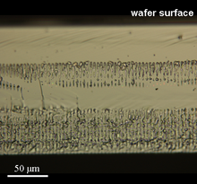
Dicing of silicon wafers may also be performed by a laser-based technique, the so-called stealth dicing process. It works as a two-stage process in which defect regions are firstly introduced into the wafer by scanning the beam along intended cutting lines and secondly an underlying carrier membrane is expanded to induce fracture.[5]
The first step operates with a pulsed
It is the advantage of the stealth dicing process that it does not require a
Dice before grind
The DBG or "dice before grind" process is a way to separate dies without dicing. The separation occurs during the wafer thinning step. The wafers are initially diced using a half-cut dicer to a depth below the final target thickness. Next, the wafer is thinned to the target thickness while mounted on a special adhesive film[9] and then mounted on to a pick-up tape to hold the dies in place until they are ready for the packaging step. The benefit to the DBG process is higher die strength.[10] Alternatively, plasma dicing may be used, which replaces the dicer's saw with DRIE plasma etching.[11][12][13][14][15][16][17][18]
The DBG process requires a back grinding tape that has the following attributes, 1) strong adhesive force (prevents infiltration of grinding fluid and die dust during grinding), 2) absorption and/or relief of compression stress and shear stress during grinding, 3) suppresses cracking due to contact between dies, 4) adhesive strength that can be greatly reduced through UV irradiation.[19]
See also
References
- ^ ISSN 2166-2746.
- ^ "Key Wafer Sawing Factors". Optocap. Archived from the original on 21 May 2013. Retrieved 14 April 2013.
- ^ "Wafer Dicing Service | Wafer Backgrinding & Bonding Services". www.syagrussystems.com. Retrieved 2021-11-20.
- ^ a b c M. Birkholz; K.-E. Ehwald; M. Kaynak; T. Semperowitsch; B. Holz; S. Nordhoff (2010). "Separation of extremely miniaturized medical sensors by IR laser dicing". J. Opto. Adv. Mat. 12: 479–483.
- S2CID 6034954.
- ^ a b E. Ohmura; F. Fukuyo; K. Fukumitsu; H. Morita (2006). "Internal modified layer formation mechanism into silicon with nanosecond laser". J. Achiev. Mat. Manuf. Eng. 17: 381–384.
- ^ S2CID 6034954.
- ^ "共通 | DISCO Corporation".
- ^ "共通 | DISCO Corporation".
- ^ "Semiconductor Dicing Tapes". Semiconductor Dicing Tapes. Retrieved 14 April 2013.
- ^ "Plasma Dicing | Orbotech". www.orbotech.com.
- ^ "APX300 : Plasma Dicer - Industrial Devices & Solutions - Panasonic". industrial.panasonic.com.
- ^ "Plasma Dicing of Silicon & III-V (GaAs, InP & GaN)". SAMCO Inc.
- ^ "Example of plasma dicing process | Download Scientific Diagram".
- ^ "Plasma-Therm: Plasma Dicing". www.plasmatherm.com. Archived from the original on 2023-03-06. Retrieved 2019-05-26.
- ^ "Plasma Dicing Solutions of a Variety of Materials: From Silicon Wafers with Metal or Resin Layers, to Compound Semiconductors" (PDF). Retrieved 2023-11-19.
- ^ "Resource Center". Plasma-Therm. June 22, 2022.
- ^ "Plasma Dicing (Dice Before Grind) | Orbotech". www.orbotech.com.
- ^ Products for DBG Process (LINTEC) http://www.lintec-usa.com/di_dbg.cfm
