
Photoresist
A photoresist (also known simply as a resist) is a light-sensitive material used in several processes, such as photolithography and photoengraving, to form a patterned coating on a surface. This process is crucial in the electronics industry.[1]
The process begins by coating a substrate with a light-sensitive organic material. A patterned mask is then applied to the surface to block light, so that only unmasked regions of the material will be exposed to light. A solvent, called a developer, is then applied to the surface. In the case of a positive photoresist, the photo-sensitive material is degraded by light and the developer will dissolve away the regions that were exposed to light, leaving behind a coating where the mask was placed. In the case of a negative photoresist, the photosensitive material is strengthened (either polymerized or cross-linked) by light, and the developer will dissolve away only the regions that were not exposed to light, leaving behind a coating in areas where the mask was not placed.

A BARC coating (Bottom Anti-Reflectant Coating) may be applied before the photoresist is applied, to avoid reflections from occurring under the photoresist and to improve the photoresist's performance at smaller semiconductor nodes.[2][3][4]
Conventional photoresists typically consist of 3 components: resin (a binder that provides physical properties such as adhesion, chemical resistance, etc), sensitizer (which has a photoactive compound), and solvent (which keeps the resist liquid).
Definitions
Simple resist polarity
Positive: light will weaken the resist, and create a hole
Negative: light will toughen the resist and create an etch resistant mask.
To explain this in graphical form you may have a graph on Log exposure energy versus fraction of resist thickness remaining. The positive resist will be completely removed at the final exposure energy and the negative resist will be completely hardened and insoluble by the end of exposure energy. The slope of this graph is the contrast ratio. Intensity (I) is related to energy by E = I*t.
Positive photoresist

A positive photoresist is a type of photoresist in which a portion is exposed to light and becomes soluble to the photoresist developer. The unexposed portion of the photoresist remains insoluble in the photoresist developer.
Some examples of positive photoresists are:
PMMA (polymethylmethacrylate) single-component
- Resist for deep-UV, e-beam, x-ray
- Resin itself is DUV sensitive (slow)
- Chain scission mechanism
Two-component DQN resists:
- Common resists for mercury lamps
- Diazoquinone ester (DQ) 20-50% weight
- photosensitive
- hydrophobic, not water soluble
- Phenolic Novolak Resin (N)
- Frequently used for near-UV exposures
- Water soluble
- UV exposure destroys the inhibitory effect of DQ
- Issues: Adhesion, Etch Resistance
Negative photoresist

A negative photoresist is a type of photoresist in which the portion of the photoresist that is exposed to light becomes insoluble in the photoresist developer. The unexposed portion of the photoresist is dissolved by the photoresist developer.
- Based on cyclized polyisoprene (rubber)
- variety of sensitizers (only a few % by weight)
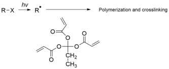
- free radical initiated photo cross-linking of polymers
- Issues:
- potential oxygen inhibition
- swelling during development
- long narrow lines can become wavy
- swelling is an issue for high-resolution patterning
- Example: SU-8 (epoxy-based polymer), good adhesion), Kodak Photoresist (KPR)
Modulation transfer function
MTF (modulation transfer function is the ratio of image intensity modulation and object intensity modulation and it is a parameter that indicates the capability of an optical system.
Differences between positive and negative resist
The following table
| Characteristic | Positive | Negative |
| Adhesion to silicon | Fair | Excellent |
| Relative cost | More expensive | Less expensive |
| Developer base | Aqueous | Organic |
| Solubility in the developer | Exposed region is soluble | Exposed region is insoluble |
| Minimum feature | 0.5 μm | 7 nm |
| Step coverage | Better | Lower |
| Wet chemical resistance | Fair | Excellent |
Classification


Based on the chemical structure of photoresists, they can be classified into three types: photopolymeric, photodecomposing, and photocrosslinking photoresist.
- allyl monomer, which could generate free radical when exposed to light, then initiates the photopolymerization of monomer to produce a polymer. Photopolymeric photoresists are usually used for negative photoresist, e.g. methyl methacrylate and poly(phthalaldehyde)/PAG blends
- Photocrosslinking photoresist is a type of photoresist, which could crosslink chain by chain when exposed to light, to generate an insoluble network. Photocrosslinking photoresist are usually used for negative photoresist.

* Photodecomposing photoresist is a type of photoresist that generates hydrophilic products under light. Photodecomposing photoresists are usually used for positive photoresist. A typical example is azide quinone, e.g. diazonaphthaquinone (DQ).
- For self-assembled monolayer SAM photoresist, first a SAM is formed on the substrate by self-assembly. Then, this surface covered by SAM is irradiated through a mask, similar to other photoresist, which generates a photo-patterned sample in the irradiated areas. And finally developer is used to remove the designed part (could be used as both positive or negative photoresist).[7]
Light sources
Absorption at UV and shorter wavelengths
In lithography, decreasing the wavelength of light source is the most efficient way to achieve higher resolution.
Electron-beam exposure
Photoresists can also be exposed by electron beams, producing the same results as exposure by light. The main difference is that while photons are absorbed, depositing all their energy at once, electrons deposit their energy gradually, and scatter within the photoresist during this process. As with high-energy wavelengths, many transitions are excited by electron beams, and heating and outgassing are still a concern. The dissociation energy for a C-C bond is 3.6 eV. Secondary electrons generated by primary ionizing radiation have energies sufficient to dissociate this bond, causing scission. In addition, the low-energy electrons have a longer photoresist interaction time due to their lower speed; essentially the electron has to be at rest with respect to the molecule in order to react most strongly via dissociative electron attachment, where the electron comes to rest at the molecule, depositing all its kinetic energy.[12] The resulting scission breaks the original polymer into segments of lower molecular weight, which are more readily dissolved in a solvent, or else releases other chemical species (acids) which catalyze further scission reactions (see the discussion on chemically amplified resists below). It is not common to select photoresists for electron-beam exposure. Electron beam lithography usually relies on resists dedicated specifically to electron-beam exposure.
Parameters
Physical, chemical, and optical properties of photoresists influence their selection for different processes.[13] The primary properties of the photoresist are resolution capability, process dose and focus latitudes required for curing, and resistance to reactive ion etching.[14]: 966 [15] Other key properties are sensitivity, compatibility with tetramethylammonium hydroxide (TMAH), adhesion, environmental stability, and shelf life.[14]: 966 [15]
- Resolution
- Resolution is the ability to differ the neighboring features on the substrate. Critical dimension (CD) is a main measure of resolution. The smaller the CD is, the higher resolution would be.
- Contrast
- Contrast is the difference from exposed portion to unexposed portion. The higher the contrast is, the more obvious the difference between exposed and unexposed portions would be.
- Sensitivity
- Sensitivity is the minimum energy that is required to generate a well-defined feature in the photoresist on the substrate, measured in mJ/cm2. The sensitivity of a photoresist is important when using deep ultraviolet (DUV) or extreme-ultraviolet (EUV).
- Viscosity
- Viscosity is a measure of the internal friction of a fluid, affecting how easily it will flow. When it is needed to produce a thicker layer, a photoresist with higher viscosity will be preferred.
- Adherence
- Adherence is the adhesive strength between photoresist and substrate. If the resist comes off the substrate, some features will be missing or damaged.
- Etching resistance
- Anti-etching is the ability of a photoresist to resist the high temperature, different pH environment or the ion bombardment in the process of post-modification.
- Surface tension
- Surface tension is the tension that induced by a liquid tended to minimize its surface area, which is caused by the attraction of the particles in the surface layer. In order to better wet the surface of substrate, photoresists are required to possess relatively low surface tension.
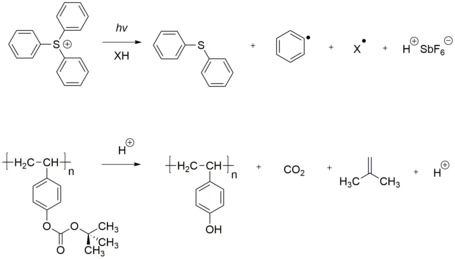
Chemical amplification
Photoresists used in production for DUV and shorter wavelengths require the use of chemical amplification to increase the sensitivity to the exposure energy. This is done in order to combat the larger absorption at shorter wavelengths. Chemical amplification is also often used in electron-beam exposures to increase the sensitivity to the exposure dose. In the process, acids released by the exposure radiation diffuse during the post-exposure bake step. These acids render surrounding polymer soluble in developer. A single acid molecule can catalyze many such 'deprotection' reactions; hence, fewer photons or electrons are needed.[16] Acid diffusion is important not only to increase photoresist sensitivity and throughput, but also to limit line edge roughness due to shot noise statistics.[17] However, the acid diffusion length is itself a potential resolution limiter.[18] In addition, too much diffusion reduces chemical contrast, leading again to more roughness.[17]
The following reactions are an example of commercial chemically amplified photoresists in use today:
- photoacid generator + hν (193 nm) → acid cation + sulfonate anion [19]
- sulfonate anion + hν (193 nm) → e− + sulfonate[20]
- e− + photoacid generator → e− + acid cation + sulfonate anion [19]
The e− represents a
Types
DNQ-Novolac photoresist
One very common positive photoresist used with the I, G and H-lines from a mercury-vapor lamp is based on a mixture of
Epoxy-based resists
One very common negative photoresist is based on epoxy-based oligomer. The common product name is SU-8 photoresist, and it was originally invented by IBM, but is now sold by Microchem and Gersteltec. One unique property of SU-8 is that it is very difficult to strip. As such, it is often used in applications where a permanent resist pattern (one that is not strippable, and can even be used in harsh temperature and pressure environments) is needed for a device.[23] Mechanism of epoxy-based polymer is shown in 1.2.3 SU-8. SU-8 is prone to swelling at smaller feature sizes, which has led to the development of small-molecule alternatives that are capable of obtaining higher resolutions than SU-8.[24]
Off-stoichiometry thiol-enes(OSTE) polymer
In 2016, OSTE Polymers were shown to possess a unique photolithography mechanism, based on diffusion-induced monomer depletion, which enables high photostructuring accuracy. The OSTE polymer material was originally invented at the KTH Royal Institute of Technology, but is now sold by Mercene Labs. Whereas the material has properties similar to those of SU8, OSTE has the specific advantage that it contains reactive surface molecules, which make this material attractive for microfluidic or biomedical applications.[13]
Hydrogen silsesquioxane (HSQ)
HSQ is a common negative resist for e-beam, but also useful for photolithography. Originally invented by Dow Corning (1970),[25] and now produced (2017) by Applied Quantum Materials Inc. (AQM). Unlike other negative resists, HSQ is inorganic and metal-free. Therefore, exposed HSQ provides a low dielectric constant (low-k) Si-rich oxide. A comparative study against other photoresists was reported in 2015 (Dow Corning HSQ).[26]
Applications


Microcontact printing
Microcontact printing was described by Whitesides Group in 1993. Generally, in this techniques, an elastomeric stamp is used to generate two-dimensional patterns, through printing the “ink” molecules onto the surface of a solid substrate.[27]
Step 1 for microcontact printing. A scheme for the creation of a polydimethylsiloxane (PDMS) master stamp. Step 2 for microcontact printing A scheme of the inking and contact process of microprinting lithography.
Printed circuit boards
The manufacture of printed circuit boards is one of the most important uses of photoresist. Photolithography allows the complex wiring of an electronic system to be rapidly, economically, and accurately reproduced as if run off a printing press. The general process is applying photoresist, exposing image to ultraviolet rays, and then etching to remove the copper-clad substrate.[28]

Patterning and etching of substrates
This includes specialty photonics materials, MicroElectro-Mechanical Systems (

Microelectronics
This application, mainly applied to

See also
References
- ^ Eric, Anslyn; Dougherty, Dennis. Modern physical organic chemistry. University Science Books.
- ^ "Top Anti-reflective Coatings vs Bottom Anti-reflective Coatings".
- ^ MicroChemicals. "Basics of Microstructuring: Anti-Reflective Coatings" (PDF). Microchemicals GmbH. Retrieved 2020-01-31.
- ^ "AR™ 10L Bottom Anti-Reflectant Coating (BARC) | DuPont". dupont.com.
- ^ Ito, H.; Willson, C. G.; Frechet, J. H. J. (1982-09-01). "New UV Resists with Negative or Positive Tone". 1982 Symposium on VLSI Technology. Digest of Technical Papers: 86–87.
- ISBN 978-0-8493-0826-0.
- ISSN 0743-7463.
- S2CID 55877239.
- S2CID 98281255.
- .
- S2CID 13859981.
- .
- ^ S2CID 24567881.
- ^ )
- ^ ISBN 978-0-387-31235-4, retrieved 2023-01-06
- ^ U.S. patent 4,491,628 "Positive and Negative Working Resist Compositions with Acid-Generating Photoinitiator and Polymer with Acid-Labile Groups Pendant From Polymer Backbone" J.M.J. Fréchet, H. Ito and C.G. Willson 1985.[1]
- ^ .
- S2CID 95710610.
- ^ S2CID 95525894.
- .
- .
- .
- ^ DeForest, William S (1975). Photoresist: materials and processes. McGraw-Hill Companies.
- S2CID 122244702.
- ISSN 0002-7863.
- PMID 25783209.
- ^ "Self-assembled Monolayer Films: Microcontact Printing" (PDF).
- ^ Montrose, Mark I (1999). The Electronic Packaging Handbook. CRC Press.
- ISBN 978-1566772594.
- ^ Silicon photonics. Springer Science & Business Media. 2004.