Northbridge (computing)
This article needs additional citations for verification. (January 2008) |


In computing, a northbridge (also host bridge, or memory controller hub) is a
Historically, separation of functions between CPU, northbridge, and southbridge chips was necessary due to the difficulty of integrating all components onto a single
On older Intel based PCs, the northbridge was also named external memory controller hub or graphics and memory controller hub if equipped with integrated graphics. Increasingly these functions became integrated into the CPU chip itself,
Overview
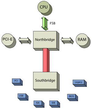
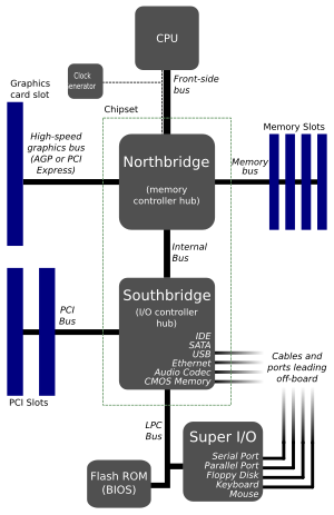
The northbridge typically handles communications among the CPU, in some cases RAM, and PCI Express (or AGP) video cards, and the southbridge.[7][8] Some northbridges also contain integrated video controllers, also known as a Graphics and Memory Controller Hub in Intel systems. Because different processors and RAM require different signaling, a given northbridge will typically work with only one or two classes of CPUs and generally only one type of RAM.
There are a few chipsets that support two types of RAM; generally, these are made available when there is a shift to a new standard. For example, the northbridge from the 2002 Nvidia nForce2 chipset only worked with Socket A processors combined with DDR SDRAM.
The Intel i875 chipset will only work with systems using Pentium 4 processors or Celeron processors that have a clock speed greater than 1.3 GHz and utilize DDR SDRAM, and the Intel i915G chipset only works with the Intel Pentium 4 and the Celeron, but it can use DDR or DDR2 memory.[citation needed]
PowerPC
Northbridge chips are most commonly found on X86-based PCs, but they can also be found on other platforms, such as the PowerPC platform. A common example of a northbridge on a PowerPC platform is in Apple's older PowerPC-based computers like the iMac G5, which utilized an IBM CPC945 Northbridge chip. According to an Apple Developer note, The Power Mac G5's northbridge chip connected to a "Mid Bridge", which then connected to a south bridge.[9]

Etymology
The name is derived from drawing the architecture in the fashion of a map. The CPU would be at the top of the map comparable to due north on most general purpose geographical maps. The CPU would be connected to the chipset via a fast bridge (the northbridge) located north of other system devices as drawn. The northbridge would then be connected to the rest of the chipset via a slow bridge (the southbridge) located south of other system devices as drawn.

Overclocking
The northbridge plays an important part in how far a computer can be
Evolution

The overall trend in processor design has been to integrate more functions onto fewer components, which decreases overall motherboard cost and improves performance. The memory controller, which handles communication between the CPU and RAM, was moved onto the processor die by AMD beginning with their AMD K8 processors and by Intel with their Nehalem processors. One of the advantages of having the memory controller integrated on the CPU die is to reduce latency from the CPU to memory.
Some northbridge chips have supported dual processors, for example Intel's 5000X memory controller used in the original Mac Pro from 2006.
Another example of this kind of change is Nvidia's nForce3 for AMD K8 systems. It combines all of the features of a normal southbridge with an Accelerated Graphics Port (AGP) port and connects directly to the CPU. On nForce4 boards it was marketed as a media communications processor (MCP).
The northbridge was replaced by the system agent introduced by the Intel
Recent AMD processors starting with the Zen 2 have moved some I/O functions out of the CPU die onto an I/O die on the same MCM package as the CPU. This die is not normally considered to be part of the Northbridge, since it is in the same package as the CPU, but it serves some of the same functions.[12]
See also
References
- ^ "Definition of:Northbridge". PC Magazine. Retrieved September 26, 2015.
- ^ "Chipset: Northbridge and Southbridge". Rigacci.org. 2006-01-27. Retrieved 2015-05-07.
- ISBN 9780824722937. Retrieved September 26, 2015.
- ^ The Macbook Air: A Sign of Things to Come – Digital Gravitas
- ^ a b "Trustworthy x86 laptops? There is a way, says system-level security ace". The Register. Retrieved January 4, 2016.
- ^ a b "Northbridge". Computer Hope. October 7, 2019.
- ^ Jones, George (2004-10-22). "Motherboards & Core-Logic Chipsets: The Deep Stuff | What the North Bridge and South Bridge Do". InformIT.com. Retrieved 2015-05-07.
- ISBN 0-7686-6312-1
- ^ "Power Mac G5 Developer Note".
- ^ "The Ring Bus & System Agent - Intel's Sandy Bridge Architecture Exposed". Anandtech.com. Retrieved 2015-05-07.
- ^ "Intel Core i5 2500K and Core i7 2600K (Sandy Bridge) - Introduction". Legionhardware.com. Archived from the original on 2016-06-05. Retrieved 2015-05-07.
- ^ "Chiplets Are the Future, but They Won't Replace Moore's Law".
