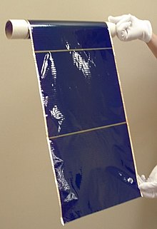
Amorphous silicon
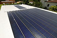
- Thin-film silicon solar panels on rooftop
- Schematic structures of hydrogenatedsilicon
- Solar calculator with amorphous solar cell (upper right corner) and LCDs.
Amorphous silicon (a-Si) is the non-
.Used as
As a second-generation
Amorphous silicon differs from other
Description
Silicon is a fourfold coordinated atom that is normally tetrahedrally bonded to four neighboring silicon atoms. In crystalline silicon (c-Si) this tetrahedral structure continues over a large range, thus forming a well-ordered crystal lattice.
In amorphous silicon this long range order is not present. Rather, the atoms form a continuous random network. Moreover, not all the atoms within amorphous silicon are fourfold coordinated. Due to the disordered nature of the material some atoms have a dangling bond. Physically, these dangling bonds represent defects in the continuous random network and may cause anomalous electrical behavior.
The material can be

Amorphous silicon and carbon
Amorphous alloys of silicon and carbon (amorphous silicon carbide, also hydrogenated, a-Si1−xCx:H) are an interesting variant. Introduction of carbon atoms adds extra degrees of freedom for control of the properties of the material. The film could also be made transparent to visible light.
Increasing the concentration of carbon in the alloy widens the electronic gap between conduction and valence bands (also called "optical gap" and
Several studies are found in the scientific literature, mainly investigating the effects of deposition parameters on electronic quality, but practical applications of amorphous silicon carbide in commercial devices are still lacking.
Properties
The density of ion implanted amorphous Si has been calculated as 4.90×10²² atom/cm3 (2.285 g/cm3) at 300 K. This was done using thin (5 micron) strips of amorphous silicon. This density is 1.8±0.1% less dense than crystalline Si at 300 K.[4] Silicon is one of the few elements that expands upon cooling and has a lower density as a solid than as a liquid.
Hydrogenated amorphous silicon
Unhydrogenated a-Si has a very high defect density which leads to undesirable semiconductor properties such as poor photoconductivity and prevents doping which is critical to engineering semiconductor properties. By introducing hydrogen during the fabrication of amorphous silicon, photoconductivity is significantly improved and doping is made possible. Hydrogenated amorphous silicon, a-Si:H, was first fabricated in 1969 by Chittick, Alexander and Sterling by deposition using a silane gas (SiH4) precursor. The resulting material showed a lower defect density and increased conductivity due to impurities. Interest in a-Si:H came when (in 1975), LeComber and Spear discovered the ability for substitutional doping of a-Si:H using phosphine (n-type) or diborane (p-type).[5] The role of hydrogen in reducing defects was verified by Paul's group at Harvard who found a hydrogen concentration of about 10 atomic % through IR vibration, which for Si-H bonds has a frequency of about 2000 cm−1.[6] Starting in the 1970s, a-Si:H was developed in solar cells by David E. Carlson and C. R. Wronski at RCA Laboratories.[7] Conversion efficiency steadily climbed to about 13.6% in 2015.[8]
Deposition processes
| CVD | PECVD | Catalytic CVD | Sputtering | |
|---|---|---|---|---|
| Type of film | a-Si:H | a-Si:H | a-Si:H | a-Si |
| Unique application | Large-area electronics
|
Hydrogen-free deposition | ||
| Chamber temperature | 600C | 30–300C | 30–1000C | |
| Active element temperature | 2000C | |||
| Chamber pressure | 0.1–10 Torr | 0.1–10 Torr | 0.001–0.1 Torr | |
| Physical principle | Thermolysis | Plasma-induced dissociation | Thermolysis | Ionization of Si source |
| Facilitators | W/Ta heated wires | Argon cations | ||
| Typical drive voltage | RF 13.56 MHz; 0.01-1W/cm2 | |||
| Si source | SiH4 gas | SiH4 gas | SiH4 gas | Target |
| Substrate temperature | controllable | controllable | controllable | controllable |
Applications
While a-Si suffers from lower electronic performance compared to c-Si, it is much more flexible in its applications. For example, a-Si layers can be made thinner than c-Si, which may produce savings on silicon material cost.
One further advantage is that a-Si can be deposited at very low temperatures, e.g., as low as 75 degrees Celsius. This allows deposition on not only glass, but on
Another advantage is that a-Si can be deposited over large areas by
Arrays of small (under 1 mm by 1 mm) a-Si photodiodes on glass are used as visible-light
Photovoltaics

Hydrogenated amorphous silicon (a-Si:H) has been used as a
More recently, improvements in a-Si:H construction techniques have made them more attractive for large-area solar cell use as well. Here their lower inherent efficiency is made up, at least partially, by their thinness – higher efficiencies can be reached by stacking several thin-film cells on top of each other, each one tuned to work well at a specific frequency of light. This approach is not applicable to c-Si cells, which are thick as a result of its indirect band-gap and are therefore largely opaque, blocking light from reaching other layers in a stack.
The source of the low efficiency of amorphous silicon photovoltaics is due largely to the low
The main advantage of a-Si:H in large scale production is not efficiency, but cost. a-Si:H cells use only a fraction of the silicon needed for typical c-Si cells, and the cost of the silicon has historically been a significant contributor to cell cost. However, the higher costs of manufacture due to the multi-layer construction have, to date, made a-Si:H unattractive except in roles where their thinness or flexibility are an advantage.[18]
Typically, amorphous silicon thin-film cells use a
Microcrystalline and micromorphous silicon
Microcrystalline silicon (also called nanocrystalline silicon) is amorphous silicon, but also contains small crystals. It absorbs a broader spectrum of light and is
Large-scale production

Photovoltaic thermal hybrid solar collectors

Thin-film-transistor liquid-crystal display
Amorphous silicon has become the material of choice for the active layer in
Polycrystalline silicon is sometimes used in displays requiring higher TFT performance. Examples include small high-resolution displays such as those found in projectors or viewfinders. Amorphous silicon-based TFTs are by far the most common, due to their lower production cost, whereas polycrystalline silicon TFTs are more costly and much more difficult to produce.[24]
See also
- Atomic layer deposition (ALD)
- Chemical-mechanical planarization(CMP)
- Chemical vapor deposition (CVD)
- Crystalline silicon
- Ion implantation
- Nanoparticle
- Physical vapor deposition (PVD)
- Protocrystalline
- Rapid thermal processing (RTP)
References
- .
- .
- doi:10.1109/16.40969.
- ISSN 0003-6951.
- ISBN 9780521019347.
- .
- doi:10.1063/1.88617.
- ^ File:PVeff(rev170324).png
- S2CID 94159781.
- ISSN 2050-7496.
- .
- S2CID 3961031.
- S2CID 18053686.
- PMID 10035845.
- PMID 9991947.
- PMID 25167024.
- hdl:1721.1/89217.
- ^ Wesoff, Eric (January 31, 2014) "The End of Oerlikon’s Amorphous Silicon Solar Saga." Greentech Media.
- ^ "The End Arrives for ECD Solar". GreentechMedia. February 14, 2012.
- ^ "Oerlikon Divests Its Solar Business and the Fate of Amorphous Silicon PV". GrrentechMedia. March 2, 2012.
- ^ "Xunlight Completes Installation of its First 25 Megawatt Wide-Web Roll-to-Roll Photovoltaic Manufacturing Equipment". Xunlight. June 22, 2009.
- ^ "Anwell Produces its First Thin Film Solar Panel". Solarbuzz. September 7, 2009.
- ^ "TFT LCD – Fabricating TFT LCD". Plasma.com. Archived from the original on May 2, 2013. Retrieved July 21, 2013.
- ^ "TFT LCD – Electronic Aspects of LCD TVs and LCD Monitors". Plasma.com. Archived from the original on August 23, 2013. Retrieved July 21, 2013.


