
Graphene lens
A graphene lens is an optical refraction device. Graphene's unique 2-D honeycomb contributes to its unique optical properties.
Graphene
The honeycomb structure allows
- (Equation 1)

-
 A representation of graphene's band gap before and after doping (Figure 1a)
 -
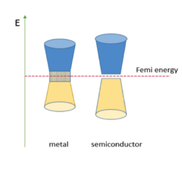 A representation of convention metal and semiconductor band gaps (Figure 1b)


This behavior is the result of an undoped graphene material at zero temperature (Figure 1a).[3] In contrast to traditional semiconductors or metals (Figure 1b); graphene's band gap is nearly nonexistent because the conducting and valence bands make contact (Figure 1a). However, the band gap is tunable via doping and electrical gating, changing optical properties.[4] As a result of its tunable conductivity, graphene is suitable for various optical applications.
Applications
Photodetectors
Electrical gating and doping allows for adjustment of graphene's optical absorptivity.[5][6] The application of electric fields transverse to staggered graphene bilayers generates a shift in Fermi energy and an artificial, non-zero band gap (Equation 2,[4] Figure 1).

- (Equation 2)

where
- Dt = top electrical displacement field
- Db = bottom electrical displacement field
Varying δD above or below zero (δD=0 denotes non-gated, neutral bilayers) allows electrons to pass through the bilayer without altering the gating-induced band gap.[7] Varying the average displacement field, ▁D, alters the bilayer's absorption spectra (as shown in Figure 2). The optical tunability resulting from gating and electrostatic doping (also known as charge plasma doping[8]) lends to the application of graphene as an ultra-broadband photodetector in lenses.[9]

Chang-Hua et al. implemented graphene in an infrared photodetector by sandwiching an insulating barrier of Ta
2O
5 between two graphene sheets.[10] The graphene layers became electrically isolated and exhibited an average Fermi difference of 0.12eV when a current was passed through the bottom layer (Figure 3). When the photodetector is exposed to light, excited hot electrons transitioned from the top graphene layer to the bottom, a process promoted by the structural asymmetry of the insulating Ta
2O
5 barrier.[9][11] As a consequence of the hot electron transition, the top layer accumulates positive charges and induces a photogating [9][12] effect on the lower graphene layer, which is measured as a change in current correlating with photon detection.[4] Utilizing graphene both as a channel for charge transport and light absorption, the photodetectors ably detects the visible to mid-infrared spectrum. Nanometers thin and functional at room temperature, graphene photodetectors show promise in lens applications.
Fresnel zone plates

Fresnel zone plates are devices that focus light on a fixed point in space. These devices concentrate light reflected off a lens onto a singular point (Figure 4). Composed of a series of discs centered about an origin, Fresnel zone plates are manufactured using laser pulses, which embed voids into a reflective lens.
Despite its weak reflectance (R = 0.25π2 α 2 at T = 1.3 × 10⁻⁴ K), graphene has utility as a lens for Fresnel zone plates.[13] Graphene lenses effectively concentrate light of ʎ = 850 nm onto a single point 120 μm away from the Fresnel zone plate[13] (Figure 5). Further investigation illustrates that the reflected intensity increases linearly with the number of graphene layers within the lens[13] (Figure 6).

Transparent conductors
- (Equation 3)

where t is the film thickness and σ is the DC conductivity.
A material with tunable thickness t and conductivity σ is suitable for
The need for alternative transparent conductors is well documented.[17][18][19] Semiconductor based transparent conductors such as doped indium oxides, zinc oxides, or tin oxides suffer from practical downfalls including rigorous processing requirements, prohibitive cost, sensitivity toward Ph, and brittle consistency. However, graphene does not suffer from these shortfalls.