Pixel Visual Core
The Pixel Visual Core (PVC) is a series of
History
Google previously used
The PVC in the
The PVC in the
Thanks to the PVC, the Pixel 2 and Pixel 3 obtained a mobile DxOMark of 98[5] and 101.[6] The latter one was the top-ranked single-lens mobile DxOMark score, tied with the iPhone XR.[7]
Pixel Visual Core software

A typical image-processing program of the PVC is written in Halide. Currently, it supports just a subset of Halide programming language without floating point operations and with limited memory access patterns.[8] Halide is a domain-specific language that lets the user decouple the algorithm and the scheduling of its execution. In this way, the developer can write a program that is optimized for the target hardware architecture.[2]
Pixel Visual Core ISA
The PVC has two types of instruction set architecture (ISA), a virtual and a physical one. First, a high-level language program is compiled into a virtual ISA (vISA), inspired by RISC-V ISA,[2] which abstracts completely from the target hardware generation. Then, the vISA program is compiled into the so-called physical ISA (pISA), that is a VLIW ISA. This compilation step takes into account the target hardware parameters (e.g. array of PEs size, STP size, etc...) and specify explicitly memory movements. The decoupling of vISA and pISA lets the first one to be cross-architecture and generation-independent, while pISA can be compiled offline or through JIT compilation.[8]
Pixel Visual Core architecture

The Pixel Visual Core is designed to be a scalable multi-core energy-efficient architecture, ranging from even numbers between 2 and 16 core designs.
Image Processing Unit (IPU)
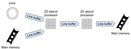
The IPU core has a stencil processor (STP), a line buffer pool (LBP) and a NoC. The STP mainly provides a 2-D
Line Buffer Pool (LBP)
Considering that one of the most energy costly operation is DRAM access, each STP has temporary buffers to increase data locality, namely LBP. The used LBP is a 2-D FIFO that accommodates different sizes of reading and writing. The LBP uses single-producer multi-consumer behavioral model. Each LBP can have eight logical LB memories and one for DMA input-output operations.[8] Due to the real high complexity of the memory system, the PVC designers state the LBP controller as one of the most challenging components.[2] The NoC used is a ring network on chip used to communicate with only neighbor cores for energy savings and pipelined computational pattern preservation.[2]
Stencil Processor (STP)

The STP has a 2-D array of PEs: for example, a 16x16 array of full PEs and four lanes of simplified PEs called "halo". The STP has a scalar processor, called scalar lane (SCL), that adds control instructions with a small instruction memory. The last component of an STP is a load store unit called sheet generator (SHG), where the sheet is the PVC memory access unit.[2]
SR3HX design summary
The SR3HX PVC features a 64-bit ARMv8a
References
- ^ a b c Cutress, Ian. "Hot Chips 2018: The Google Pixel Visual Core Live Blog (10am PT, 5pm UTC)". www.anandtech.com. Retrieved 2019-02-02.
- ^ ISBN 978-0-12-811905-1.
- ^ "Google Pixel 2 XL Teardown". iFixit. 2017-10-19. Retrieved 2019-02-02.
- ^ "Google Pixel 3 XL Teardown". iFixit. 2018-10-16. Retrieved 2019-02-02.
- ^ "Pixel 2 DxOMark".
- ^ "Pixel 3 DxOMark".
- ^ "iPhone XR DxOMark".
- ^ a b c d "The Pixel Visual Core: Google's Fully Programmable Image, Vision and AI Processor for Mobile Devices. HotChips2018" (PDF).
- ^ "Pixel Visual Core (PVC) - Google - WikiChip". en.wikichip.org. Retrieved 2019-02-02.
- ^ "Google Partnered with Intel for the Pixel Visual Core Chip in the Pixel 2". xda-developers. 2017-10-25. Retrieved 2019-02-02.
- ^ a b "Pixel Visual Core: image processing and machine learning on Pixel 2". Google. 2017-10-17. Retrieved 2019-02-02.
