Superlattice
A superlattice is a
Discovery
Superlattices were discovered early in 1925 by Johansson and Linde[1] after the studies on gold-copper and palladium-copper systems through their special X-ray diffraction patterns. Further experimental observations and theoretical modifications on the field were done by Bradley and Jay,[2] Gorsky,[3] Borelius,[4] Dehlinger and Graf,[5] Bragg and Williams[6] and Bethe.[7] Theories were based on the transition of arrangement of atoms in crystal lattices from disordered state to an ordered state.
Mechanical properties
J.S. Koehler theoretically predicted
The increased mechanical hardness of such superlattice materials was confirmed firstly by Lehoczky in 1978 on Al-Cu and Al-Ag,[9] and later on by several others, such as Barnett and Sproul[10] on hard PVD coatings.
Semiconductor properties
If the superlattice is made of two semiconductor materials with different
Semiconductor superlattice types
Superlattice miniband structures depend on the
Another class of quasiperiodic superlattices is named after Fibonacci. A Fibonacci superlattice can be viewed as a one-dimensional quasicrystal, where either electron hopping transfer or on-site energy takes two values arranged in a Fibonacci sequence.
Semiconductor materials

Semiconductor materials, which are used to fabricate the superlattice structures, may be divided by the element groups, IV, III-V and II-VI. While group III-V semiconductors (especially GaAs/AlxGa1−xAs) have been extensively studied, group IV heterostructures such as the SixGe1−x system are much more difficult to realize because of the large lattice mismatch. Nevertheless, the strain modification of the subband structures is interesting in these quantum structures and has attracted much attention.
In the GaAs/AlAs system both the difference in lattice constant between GaAs and AlAs and the difference of their thermal expansion coefficient are small. Thus, the remaining strain at room temperature can be minimized after cooling from
A
Production
Superlattices can be produced using various techniques, but the most common are
3) and phosphine (PH
3) have been developed.
Generally speaking MBE is a method of using three temperatures in binary systems, e.g., the substrate temperature, the source material temperature of the group III and the group V elements in the case of III-V compounds.
The structural quality of the produced superlattices can be verified by means of

Miniband structure
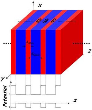
The schematic structure of a periodic superlattice is shown below, where A and B are two semiconductor materials of respective layer thickness a and b (period: ). When a and b are not too small compared with the interatomic spacing, an adequate approximation is obtained by replacing these fast varying potentials by an effective potential derived from the band structure of the original bulk semiconductors. It is straightforward to solve 1D Schrödinger equations in each of the individual layers, whose solutions are linear combinations of real or imaginary exponentials.
For a large barrier thickness, tunneling is a weak perturbation with regard to the uncoupled dispersionless states, which are fully confined as well. In this case the dispersion relation , periodic over with over by virtue of the Bloch theorem, is fully sinusoidal:
and the effective mass changes sign for :
In the case of minibands, this sinusoidal character is no longer preserved. Only high up in the miniband (for wavevectors well beyond ) is the top actually 'sensed' and does the effective mass change sign. The shape of the miniband dispersion influences miniband transport profoundly and accurate dispersion relation calculations are required given wide minibands. The condition for observing single miniband transport is the absence of interminiband transfer by any process. The thermal quantum kBT should be much smaller than the energy difference between the first and second miniband, even in the presence of the applied electric field.
Bloch states
For an ideal superlattice a complete set of
- .
As and are periodic functions with the superlattice period d, the eigenstates are
- .
Now, will exhibit a larger probability in the well, so that it seems reasonable to replace the second term by
where is the effective mass of the quantum well.
Wannier functions
By definition the
Wannier–Stark ladder
Applying an electric field F to the superlattice structure causes the Hamiltonian to exhibit an additional scalar potential eφ(z) = −eFz that destroys the translational invariance. In this case, given an eigenstate with wavefunction and energy , then the set of states corresponding to wavefunctions are eigenstates of the Hamiltonian with energies Ej = E0 − jeFd. These states are equally spaced both in energy and real space and form the so-called Wannier–Stark ladder. The potential is not bounded for the infinite crystal, which implies a continuous energy spectrum. Nevertheless, the characteristic energy spectrum of these Wannier–Stark ladders could be resolved experimentally.
Transport

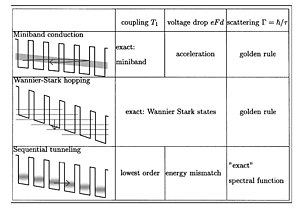
The motion of charge carriers in a superlattice is different from that in the individual layers: mobility of charge carriers can be enhanced, which is beneficial for high-frequency devices, and specific optical properties are used in semiconductor lasers.
If an external bias is applied to a conductor, such as a metal or a semiconductor, typically an electric current is generated. The magnitude of this current is determined by the band structure of the material, scattering processes, the applied field strength and the equilibrium carrier distribution of the conductor.
A particular case of superlattices called superstripes are made of superconducting units separated by spacers. In each miniband the superconducting order parameter, called the superconducting gap, takes different values, producing a multi-gap, or two-gap or multiband superconductivity.
Recently, Felix and Pereira investigated the thermal transport by phonons in periodic[13] and quasiperiodic[14][15][16] superlattices of graphene-hBN according to the Fibonacci sequence. They reported that the contribution of coherent thermal transport (phonons like-wave) was suppressed as quasiperiodicity increased.
Other dimensionalities
Soon after two-dimensional electron gases (
The difference is in the length and energy scales. Lattice constants of atomic crystals are of the order of 1Å while those of superlattices (a) are several hundreds or thousands larger as dictated by technological limits (e.g. electron-beam lithography used for the patterning of the heterostructure surface). Energies are correspondingly smaller in superlattices. Using the simple quantum-mechanically confined-particle model suggests . This relation is only a rough guide and actual calculations with currently topical graphene (a natural atomic crystal) and artificial graphene[18] (superlattice) show that characteristic band widths are of the order of 1 eV and 10 meV, respectively. In the regime of weak modulation (), phenomena like commensurability oscillations or fractal energy spectra (Hofstadter butterfly) occur.
Artificial two-dimensional crystals can be viewed as a 2D/2D case (2D modulation of a 2D system) and other combinations are experimentally available: an array of quantum wires (1D/2D) or 3D/3D photonic crystals.
Applications
The superlattice of palladium-copper system is used in high performance alloys to enable a higher electrical conductivity, which is favored by the ordered structure. Further alloying elements like silver, rhenium, rhodium and ruthenium are added for better mechanical strength and high temperature stability. This alloy is used for probe needles in probe cards.[19]
See also
- Cu-Pt type ordering in III-V semiconductor
- Tube-based nanostructures
- Wannier function
References
- .
- .
- S2CID 121876817.
- .
- S2CID 99550940.
- .
- .
- .
- ^ Lehoczky, S. L. (1973). "Retardation of dislocation generation and motion in thin-layered metal laminates". Acta Metallurgica. 41 (26): 1814.
- ISSN 0734-2101.
- .
- S2CID 2795431.
- PMID 29426893.
- S2CID 210116531.
- S2CID 245712349.
- ^ Félix, Isaac de Macêdo (4 August 2020). "Condução de calor em nanofitas quase-periódicas de grafeno-hBN" (in Brazilian Portuguese).
- doi:10.1063/1.881355.
- S2CID 119289481.
- ^ "United States Patent US10385424B2 Palladium-based alloys" (PDF). google patents. Retrieved 19 June 2020.
- H.T. Grahn, "Semiconductor Superlattices", World Scientific (1995). ISBN 978-981-02-2061-7
- Schuller, I. (1980). "New Class of Layered Materials". Physical Review Letters. 44 (24): 1597–1600. .
- Morten Jagd Christensen, "Epitaxy, Thin Films and Superlattices", Risø National Laboratory, (1997).
- C. Hamaguchi, "Basic Semiconductor Physics", Springer (2001). Superlattice at ISBN 3540416390
- Wacker, A. (2002). "Semiconductor superlattices: A model system for nonlinear transport". Physics Reports. 357 (1): 1–7. S2CID 118885849.
- Haugan, H. J.; Szmulowicz, F.; Mahalingam, K.; Brown, G. J.; Munshi, S. R.; Ullrich, B. (2005). "Short-period InAs/GaSb type-II superlattices for mid-infrared detectors". Applied Physics Letters. 87 (26): 261106. ]
Further reading
- Mendez, E. E.; doi:10.1063/1.881353.


