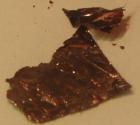
Gallium(II) selenide

| |

| |
| Names | |
|---|---|
| IUPAC name
Gallium selenide
| |
| Other names
Gallium monoselenide
| |
| Identifiers | |
3D model (
JSmol ) |
|
| ChemSpider | |
ECHA InfoCard
|
100.031.523 |
PubChem CID
|
|
| |
| |
| Properties | |
| GaSe | |
| Molar mass | 148.69 g/mol |
| Appearance | brown solid |
| Density | 5.03 g/cm3 |
| Melting point | 960 °C (1,760 °F; 1,230 K) |
| Band gap | 2.1 eV ( indirect )
|
Refractive index (nD)
|
2.6 |
| Structure | |
| hexagonal, hP8 | |
| P63/mmc, No. 194 | |
| Related compounds | |
Other anions
|
Gallium(II) oxide, Gallium(II) sulfide, Gallium(II) telluride |
Other cations
|
Zinc(II) selenide, Germanium monoselenide, Indium monoselenide
|
Related compounds
|
Gallium(III) selenide |
Except where otherwise noted, data are given for materials in their standard state (at 25 °C [77 °F], 100 kPa).
| |
Gallium(II) selenide (
Uses
It is said to have potential for optical applications
Several methods of frequency conversion using
One original problem with using gallium selenide in optics is that it is easily broken along cleavage lines and thus it can be hard to cut for practical application. It has been found, however, that
Single layers of gallium selenide are dynamically stable two-dimensional semiconductors, in which the valence band has an inverted Mexican-hat shape, leading to a Lifshitz transition as the hole-doping is increased.[9]
The integration of gallium selenide into electronic devices has been hindered by its air sensitivity. Several approaches have been developed to encapsulate GaSe mono- and few-layers, leading to improved chemical stability and electronic mobility.[10][11][12]
Synthesis
Synthesis of GaSe nanoparticles is carried out by the reaction of GaMe3 with trioctylphosphine selenium (TOPSe) in a high temperature solution of trioctylphosphine (TOP) and trioctylphosphine oxide (TOPO).[13]
- GaMe3 + P[(CH2)7CH3]3Se → GaSe
A solution of 15 g TOPO and 5 mL TOP is heated to 150 °C overnight under nitrogen, removing any water that may be present in the original TOP solution. This initial TOP solution is vacuum distilled at 0.75 torr, taking the fraction from 204 °C to 235 °C. A TOPSe solution (12.5 mL TOP with 1.579 g TOPSe) is then added and the TOPO/TOP/TOPSe reaction mixture is heated to 278 °C. GaMe3 (0.8 mL) dissolved in 7.5 mL distilled TOP is then injected. After injection, the temperature drops to 254 °C before stabilizing in the range of 266–268 °C after 10 minutes. GaSe nanoparticles then begin to form, and may be detected by a shoulder in the optical absorption spectrum in the 400–450 nm range. After this shoulder is observed, the reaction mixture is left to cool to room temperature to prevent further reaction. After synthesis and cooling, the reaction vessel is opened and extraction of the GaSe nanoparticle solution is accomplished by addition of methanol. The distribution of nanoparticles between the polar (methanol) and non-polar (TOP) phases depends on experimental conditions. If the mixture is very dry, nanoparticles partition into the methanol phase. If the nanoparticles are exposed to air or water, however, the particles become uncharged and become partitioned into the non-polar TOP phase.[13]
References
- ISBN 978-0-08-037941-8.
- .
- PMID 19876154.
- .
- ISBN 3-540-24110-8.
- .
- ^ .
- .
- S2CID 59569448.
- S2CID 204884014.
- ISSN 2567-3165.
- ^ Arora, Himani (2020). "Charge transport in two-dimensional materials and their electronic applications" (PDF). Doctoral Dissertation. Retrieved July 1, 2021.
- ^ .
