Tungsten diselenide
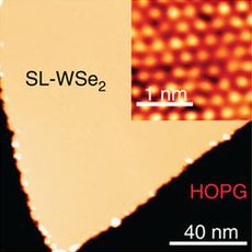
 WSe2 monolayer on graphene (yellow) and its atomic image (inset)[1]
| |

| |
| Identifiers | |
|---|---|
3D model (
JSmol ) |
|
ECHA InfoCard
|
100.031.877 |
| EC Number |
|
PubChem CID
|
|
CompTox Dashboard (EPA)
|
|
| |
| |
| Properties | |
| WSe2 | |
| Molar mass | 341.76 g/mol |
| Appearance | grey to black solid |
| Odor | odorless |
| Density | 9.32 g/cm3[2] |
| Melting point | > 1200 °C |
| insoluble | |
| Band gap | ~1 eV (indirect, bulk)[3] ~1.7 eV (direct, monolayer)[4] |
| Structure | |
| hP6, space group P6 3/mmc, No 194[2] | |
a = 0.3297 nm, c = 1.2982 nm
| |
Trigonal prismatic (WIV)Pyramidal (Se2−) | |
| Thermochemistry | |
Std enthalpy of (ΔfH⦵298)formation |
-185.3 kJ mol−1[5] |
| Hazards | |
| Occupational safety and health (OHS/OSH): | |
Main hazards
|
External MSDS |
| Related compounds | |
Other anions
|
Tantalum diselenide |
Except where otherwise noted, data are given for materials in their standard state (at 25 °C [77 °F], 100 kPa).
| |
Tungsten diselenide is an
Structure and properties
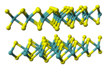
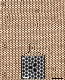
The hexagonal (P63/mmc) polymorph 2H-WSe2 is isotypic with hexagonal MoS2. The two-dimensional lattice structure has W and Se arranged periodically in layers with hexagonal symmetry. Similar to graphite, van der Waals interactions hold the layers together; however, the 2D-layers in WSe2 are not atomically thin. The large size of the W cation renders the lattice structure of WSe2 more sensitive to changes than MoS2.[8]
In addition to the typical semiconducting hexagonal structure, a second metallic polymorph of WSe2 exists. This phasem 1T-WSe2, is based on a tetragonal symmetry with one WSe2 layer per repeating unit. The 1T-WSe2 phase is less stable and transitions to the 2H-WSe2 phase.[8][9] WSe2 can form a fullerene-like structure.
The
Synthesis
Heating thin films of tungsten under pressure from gaseous selenium and high temperatures (>800 K) using the sputter deposition technique leads to the films crystallizing in hexagonal structures with the correct stoichiometric ratio.[11]
- W + 2 Se → WSe2
Potential applications

The potential applications of
2 photoelectrodes are stable in both acidic and basic conditions, making them potentially useful in electrochemical solar cells.[15][16][17]
The properties of WSe
2 monolayers differ from those of the bulk state, as is typical for semiconductors. Mechanically exfoliated monolayers of WSe
2 are transparent photovoltaic materials with LED properties.[18] The resulting solar cells pass 95 percent of the incident light, with one tenth of the remaining five percent converted into electrical power.[19][20] The material can be changed from p-type to n-type by changing the voltage of an adjacent metal electrode from positive to negative, allowing devices made from it to have tunable bandgaps.[21]
See also
References
- PMID 26179885.
- ^ .
- PMID 28191930.
- .
- .
- ISBN 0-12-352651-5
- .
- ^ ISSN 2050-7488.
- PMID 26125321.
- S2CID 231719536.
- .
- PMID 25832503.
- S2CID 124091327.
- .
- .
- S2CID 14682447.
- S2CID 3215062.
- PMID 24697842.
- ^ "Tungsten diselenide shows potential for ultrathin, flexible, semi-transparent solar cells". Gizmag.com. 11 March 2014. Retrieved 17 August 2014.
- ^ Florian Aigenr (10 March 2014). "Atomically thin solar cells" (Press release). Vienna University of Technology. Retrieved 18 August 2014.
- S2CID 224896469.
