
Electron backscatter diffraction

Electron backscatter diffraction (EBSD) is a
The change and sharpness of the electron backscatter patterns (EBSPs) provide information about lattice distortion in the diffracting volume. Pattern sharpness can be used to assess the level of plasticity. Changes in the EBSP zone axis position can be used to measure the residual stress and small lattice rotations. EBSD can also provide information about the density of geometrically necessary dislocations (GNDs). However, the lattice distortion is measured relative to a reference pattern (EBSP0). The choice of reference pattern affects the measurement precision; e.g., a reference pattern deformed in tension will directly reduce the tensile strain magnitude derived from a high-resolution map while indirectly influencing the magnitude of other components and the spatial distribution of strain. Furthermore, the choice of EBSP0 slightly affects the GND density distribution and magnitude.[1]
Pattern formation and collection
Setup geometry and pattern formation
For electron backscattering diffraction microscopy, a flat polished crystalline specimen is usually placed inside the microscope chamber. The sample is tilted at ~70° from Scanning electron microscope (SEM) flat specimen positioning and 110° to the electron backscatter diffraction (EBSD) detector.[3] Tilting the sample elongates the interaction volume perpendicular to the tilt axis, allowing more electrons to leave the sample providing better signal.[4][5] A high-energy electron beam (typically 20 kV) is focused on a small volume and scatters with a spatial resolution of ~20 nm at the specimen surface.[6] The spatial resolution varies with the beam energy,[6] angular width,[7] interaction volume,[8] nature of the material under study,[6] and, in transmission Kikuchi diffraction (TKD), with the specimen thickness;[9] thus, increasing the beam energy increases the interaction volume and decreases the spatial resolution.[10]
The EBSD detector is located within the specimen chamber of the SEM at an angle of approximately 90° to the pole piece. The EBSD detector is typically a phosphor screen that is excited by the backscattered electrons.[11] The screen is coupled to lens which focuses the image from the phosphor screen onto a charge-coupled device (CCD) or complementary metal–oxide–semiconductor (CMOS) camera.[12]
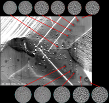
In this configuration, as the backscattered electrons leave the sample, they interact with the Coulomb potential and also lose energy due to inelastic scattering leading to a range of scattering angles (θhkl).[11][13] The backscattered electrons form Kikuchi lines – having different intensities – on an electron-sensitive flat film/screen (commonly phosphor), gathered to form a Kikuchi band. These Kikuchi lines are the trace of a hyperbola formed by the intersection of Kossel cones with the plane of the phosphor screen. The width of a Kikuchi band is related to the scattering angles and, thus, to the distance dhkl between lattice planes with Miller indexes h, k, and l.[14][15] These Kikuchi lines and patterns were named after Seishi Kikuchi, who, together with Shoji Nishikawa, was the first to notice this diffraction pattern in 1928 using transmission electron microscopy (TEM)[16] which is similar in geometry to X-ray Kossel pattern.[17][18]
The systematically arranged Kikuchi bands, which have a range of intensity along their width, intersect around the centre of the regions of interest (ROI), describing the probed volume crystallography.[19] These bands and their intersections form what is known as Kikuchi patterns or electron backscatter patterns (EBSPs). To improve contrast, the patterns’ background is corrected by removing anisotropic/inelastic scattering using static background correction or dynamic background correction.[20]

EBSD detectors
EBSD is conducted using an SEM equipped with an EBSD detector containing at least a phosphor screen, compact lens and low-light Charge-coupled device (CCD) or Complementary metal–oxide–semiconductor (CMOS) camera. As of September 2023[update], commercially available EBSD systems typically come with one of two different CCD cameras: for fast measurements, the CCD chip has a native resolution of 640×480 pixels; for slower, and more sensitive measurements, the CCD chip resolution can go up to 1600×1200 pixels.[13][6]
The biggest advantage of the high-resolution detectors is their higher sensitivity, and therefore the information within each diffraction pattern can be analysed in more detail. For texture and orientation measurements, the diffraction patterns are binned to reduce their size and computational times. Modern CCD-based EBSD systems can index patterns at a speed of up to 1800 patterns/second. This enables rapid and rich microstructural maps to be generated.[14][21]
Sample preparation
The sample should be
Inside the SEM, the size of the measurement area determines local resolution and measurement time.[26] Usual settings for high-quality EBSPs are 15 nA current, 20 kV beam energy, 18 mm working distance, long exposure time, and minimal CCD pixel binning.[27][28][29][30] The EBSD phosphor screen is set at an 18 mm working distance and a map's step size of less than 0.5 µm for strain and dislocations density analysis.[31][22]
Decomposition of gaseous hydrocarbons and also hydrocarbons on the surface of samples by the electron beam inside the microscope results in carbon deposition,[32] which degrades the quality of EBSPs inside the probed area compared to the EBSPs outside the acquisition window. The gradient of pattern degradation increases moving inside the probed zone with an apparent accumulation of deposited carbon. The black spots from the beam instant-induced carbon deposition also highlight the immediate deposition even if agglomeration did not happen.[33][34]
Depth resolution

There is no agreement about the definition of depth resolution. For example, it can be defined as the depth where ~92% of the signal is generated,[35][36] or defined by pattern quality,[37] or can be as ambiguous as "where useful information is obtained".[38] Even for a given definition, depth resolution increases with electron energy and decreases with the average atomic mass of the elements making up the studied material: for example, it was estimated as 40 nm for Si and 10 nm for Ni at 20 kV energy.[39] Unusually small values were reported for materials whose structure and composition vary along the thickness. For example, coating monocrystalline silicon with a few nm of amorphous chromium reduces the depth resolution to a few nm at 15 kV energy.[37] In contrast, Isabell and David[40] concluded that depth resolution in homogeneous crystals could also extend up to 1 µm due to inelastic scattering (including tangential smearing and channelling effect).[24]
A recent comparison between reports on EBSD depth resolution, Koko et al[24] indicated that most publications do not present a rationale for the definition of depth resolution, while not including information on the beam size, tilt angle, beam-to-sample and sample-to-detector distances.[24] These are critical parameters for determining or simulating the depth resolution.[40] The beam current is generally not considered to affect the depth resolution in experiments or simulations. However, it affects the beam spot size and signal-to-noise ratio, and hence, indirectly, the details of the pattern and its depth information.[41][42][43]
Monte Carlo simulations provide an alternative approach to quantifying the depth resolution for EBSPs formation, which can be estimated using the Bloch wave theory, where backscattered primary electrons – after interacting with the crystal lattice – exit the surface, carrying information about the crystallinity of the volume interacting with the electrons.[44] The backscattered electrons (BSE) energy distribution depends on the material's characteristics and the beam conditions.[45] This BSE wave field is also affected by the thermal diffuse scattering process that causes incoherent and inelastic (energy loss) scattering – after the elastic diffraction events – which does not, yet, have a complete physical description that can be related to mechanisms that constitute EBSP depth resolution.[46][47]
Both the EBSD experiment and simulations typically make two assumptions: that the surface is pristine and has a homogeneous depth resolution; however, neither of them is valid for a deformed sample.[37]
Orientation and phase mapping
Pattern indexing
If the setup geometry is well described, it is possible to relate the bands present in the diffraction pattern to the underlying crystal and crystallographic orientation of the material within the electron interaction volume. Each band can be indexed individually by the Miller indices of the diffracting plane which formed it. In most materials, only three bands/planes intersect and are required to describe a unique solution to the crystal orientation (based on their interplanar angles). Most commercial systems use look-up tables with international crystal databases to index. This crystal orientation relates the orientation of each sampled point to a reference crystal orientation.[3][48]
Indexing is often the first step in the EBSD process after pattern collection. This allows for the identification of the crystal orientation at the single volume of the sample from where the pattern was collected.[49][50] With EBSD software, pattern bands are typically detected via a mathematical routine using a modified Hough transform, in which every pixel in Hough space denotes a unique line/band in the EBSP. The Hough transform enables band detection, which is difficult to locate by computer in the original EBSP. Once the band locations have been detected, it is possible to relate these locations to the underlying crystal orientation, as angles between bands represent angles between lattice planes. Thus, an orientation solution can be determined when the position/angles between three bands are known. In highly symmetric materials, more than three bands are typically used to obtain and verify the orientation measurement.[50]
The diffraction pattern is pre-processed to remove noise, correct for detector distortions, and normalise the intensity. Then, the pre-processed diffraction pattern is compared to a library of reference patterns for the material being studied. The reference patterns are generated based on the material's known crystal structure and the crystal lattice's orientation. The orientation of the crystal lattice that would generate the best match to the measured pattern is determined using a variety of algorithms. There are three leading methods of indexing that are performed by most commercial EBSD software: triplet voting;[51][52] minimising the 'fit' between the experimental pattern and a computationally determined orientation,[53][54] and or/and neighbour pattern averaging and re-indexing, NPAR[55]). Indexing then give a unique solution to the single crystal orientation that is related to the other crystal orientations within the field-of-view.[56][57]
Triplet voting involves identifying multiple 'triplets' associated with different solutions to the crystal orientation; each crystal orientation determined from each triplet receives one vote. Should four bands identify the same crystal orientation, then four (four choose three, i.e. ) votes will be cast for that particular solution. Thus the candidate orientation with the highest number of votes will be the most likely solution to the underlying crystal orientation present. The number of votes for the solution chosen compared to the total number of votes describes the confidence in the underlying solution. Care must be taken in interpreting this 'confidence index' as some pseudo-symmetric orientations may result in low confidence for one candidate solution vs another.[58][59][60] Minimising the fit involves starting with all possible orientations for a triplet. More bands are included, which reduces the number of candidate orientations. As the number of bands increases, the number of possible orientations converges ultimately to one solution. The 'fit' between the measured orientation and the captured pattern can be determined.[57]

Overall, indexing diffraction patterns in EBSD involves a complex set of algorithms and calculations, but is essential for determining the crystallographic structure and orientation of materials at a high spatial resolution. The indexing process is continually evolving, with new algorithms and techniques being developed to improve the accuracy and speed of the process. Afterwards, a confidence index is calculated to determine the quality of the indexing result. The confidence index is based on the match quality between the measured and reference patterns. In addition, it considers factors such as noise level, detector resolution, and sample quality.[50]
While this geometric description related to the
Pattern centre
To relate the orientation of a crystal, much like in
Unfortunately, each of these methods is cumbersome and can be prone to some systematic errors for a general operator. Typically they cannot be easily used in modern SEMs with multiple designated uses. Thus, most commercial EBSD systems use the indexing algorithm combined with an iterative movement of crystal orientation and suggested pattern centre location. Minimising the fit between bands located within experimental patterns and those in look-up tables tends to converge on the pattern centre location to an accuracy of ~0.5–1% of the pattern width.[21][6]
The recent development of AstroEBSD[63] and PCGlobal,[64] open-source MATLAB codes, increased the precision of determining the pattern centre (PC) and – consequently – elastic strains[65] by using a pattern matching approach[66] which simulates the pattern using EMSoft.[67]
EBSD mapping

The indexing results are used to generate a map of the crystallographic orientation at each point on the surface being studied. Thus, scanning the electron beam in a prescribed fashion (typically in a square or hexagonal grid, correcting for the image foreshortening due to the sample tilt) results in many rich microstructural maps.[68][69] These maps can spatially describe the crystal orientation of the material being interrogated and can be used to examine microtexture and sample morphology. Some maps describe grain orientation, boundary, and diffraction pattern (image) quality. Various statistical tools can measure the average misorientation, grain size, and crystallographic texture. From this dataset, numerous maps, charts and plots can be generated.[70][71][72] The orientation data can be visualised using a variety of techniques, including colour-coding, contour lines, and pole figures.[73]
Microscope misalignment, image shift, scan distortion that increases with decreasing magnification, roughness and contamination of the specimen surface, boundary indexing failure and detector quality can lead to uncertainties in determining the crystal orientation.[74] The EBSD signal-to-noise ratio depends on the material and decreases at excessive acquisition speed and beam current, thereby affecting the angular resolution of the measurement.[74]
Strain measurement
Full-field displacement, elastic strain, and the GND density provide quantifiable information about the material's elastic and plastic behaviour at the microscale. Measuring strain at the microscale requires careful consideration of other key details besides the change in length/shape (e.g., local texture, individual grain orientations). These micro-scale features can be measured using different techniques, e.g., hole drilling, monochromatic or polychromatic energy-dispersive X-ray diffraction or neutron diffraction (ND). EBSD has a high spatial resolution and is relatively sensitive and easy to use compared to other techniques.[72][75][76] Strain measurements using EBSD can be performed at a high spatial resolution, allowing researchers to study the local variation in strain within a material.[14] This information can be used to study the deformation and mechanical behaviour of materials,[77] to develop models of material behaviour under different loading conditions, and to optimise the processing and performance of materials. Overall, strain measurement using EBSD is a powerful tool for studying the deformation and mechanical behaviour of materials, and is widely used in materials science and engineering research and development.[76][14]
Earlier trials
The change and degradation in electron backscatter patterns (EBSPs) provide information about the diffracting volume. Pattern degradation (i.e., diffuse quality) can be used to assess the level of plasticity through the pattern/image quality (IQ),[78] where IQ is calculated from the sum of the peaks detected when using the conventional Hough transform. Wilkinson[79] first used the changes in high-order Kikuchi line positions to determine the elastic strains, albeit with low precision[note 1] (0.3% to 1%); however, this approach cannot be used for characterising residual elastic strain in metals as the elastic strain at the yield point is usually around 0.2%. Measuring strain by tracking the change in the higher-order Kikuchi lines is practical when the strain is small, as the band position is sensitive to changes in lattice parameters.[43] In the early 1990s, Troost et al.[80] and Wilkinson et al.[81][82] used pattern degradation and change in the zone axis position to measure the residual elastic strains and small lattice rotations with a 0.02% precision.[1]
High-resolution electron backscatter diffraction (HR-EBSD)
Cross-correlation-based, high angular resolution electron backscatter diffraction (HR-EBSD) – introduced by Wilkinson et al.
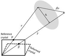
The displacement gradient tensor () (or local lattice distortion) relates the measured geometrical shifts in the pattern between the collected point () and associate (non-coplanar) vector (), and reference point () pattern and associate vector (). Thus, the (pattern shift) vector () can be written as in the equations below, where and are the direction and displacement in th direction, respectively.[87]


The shifts are measured in the phosphor (detector) plane (), and the relationship is simplified; thus, eight out of the nine displacement gradient tensor components can be calculated by measuring the shift at four distinct, widely spaced regions on the EBSP.[84][87] This shift is then corrected to the sample frame (flipped around Y-axis) because EBSP is recorded on the phosphor screen and is inverted as in a mirror. They are then corrected around the X-axis by 24° (i.e., 20° sample tilt plus ≈4° camera tilt and assuming no angular effect from the beam movement[21]). Using infinitesimal strain theory, the deformation gradient is then split into elastic strain (symmetric part, where ), and lattice rotations (asymmetric part, where ), .[84]


These measurements do not provide information about the volumetric/hydrostatic strain tensors. By imposing a boundary condition that the stress normal to the surface () is zero (i.e., traction-free surface[88]), and using Hooke's law with anisotropic elastic stiffness constants, the missing ninth degree of freedom can be estimated in this constrained minimisation problem by using a nonlinear solver.[84]


Where is the crystal anisotropic stiffness tensor. These two equations are solved to re-calculate the refined elastic deviatoric strain (), including the missing ninth (spherical) strain tensor. An alternative approach that considers the full can be found in.[88]


Finally, the stress and strain tensors are linked using the crystal anisotropic stiffness tensor (), and by using the


The quality of the produced data can be assessed by taking the geometric mean of all the ROI's correlation intensity/peaks. A value lower than 0.25 should indicate problems with the EBSPs' quality.[87] Furthermore, the geometrically necessary dislocation (GND) density can be estimated from the HR-EBSD measured lattice rotations by relating the rotation axis and angle between neighbour map points to the dislocation types and densities in a material using Nye's tensor.[31][89][90]
Precision and development
The HR-EBSD method can achieve a precision of ±10−4 in components of the displacement gradient tensors (i.e., variations in lattice strain and lattice rotation in radians) by measuring the shifts of zone axes within the pattern image with a resolution of ±0.05 pixels.[84][91] It was limited to small strains and rotations (>1.5°) until Britton and Wilkinson[86] and Maurice et al.[92] raised the rotation limit to ~11° by using a re-mapping technique that recalculated the strain after transforming the patterns with a rotation matrix () calculated from the first cross-correlation iteration.[1]


However, further lattice rotation, typically caused by severe plastic deformations, produced errors in the elastic strain calculations. To address this problem, Ruggles et al.[94] improved the HR-EBSD precision, even at 12° of lattice rotation, using the inverse compositional Gauss–Newton-based (ICGN) method instead of cross-correlation. For simulated patterns, Vermeij and Hoefnagels[95] also established a method that achieves a precision of ±10−5 in the displacement gradient components using a full-field integrated digital image correlation (IDIC) framework instead of dividing the EBSPs into small ROIs. Patterns in IDIC are distortion-corrected to negate the need for re-mapping up to ~14°.[96][97]
| Conventional EBSD | HR-EBSD | |
|---|---|---|
| Absolute orientation | 2° | N/A |
| Misorientation | 0.1° to 0.5° | 0.006° (1×10⁻⁴ rad) |
| GND @ 1 µm step
In lines/m2 (b = 0.3 nm) |
> 3×10¹³ | > 3×10¹¹ |
| Relative residual strain | N/A | Deviatoric elastic strain 1×10⁻⁴ |
| Example tasks | Texture, microstructure, etc. | Deformation |
These measurements do not provide information about the hydrostatic or
The reference pattern problem
In HR-EBSD analysis, the lattice distortion field is calculated relative to a reference pattern or point (EBSP0) per grain in the map, and is dependent on the lattice distortion at the point. The lattice distortion field in each grain is measured with respect to this point; therefore, the absolute lattice distortion at the reference point (relative to the unstrained crystal) is excluded from the HR-EBSD elastic strain and rotation maps. The local lattice distortion at the EBSP0 influences the resultant HR-EBSD map, e.g., a reference pattern deformed in tension will directly reduce the HR-EBSD map tensile strain magnitude while indirectly influencing the other component magnitude and the strain's spatial distribution. Furthermore, the choice of EBSP0 slightly affects the GND density distribution and magnitude, and choosing a reference pattern with a higher GND density reduces the cross-correlation quality, changes the spatial distribution and induces more errors than choosing a reference pattern with high lattice distortion. Additionally, there is no apparent connection between EBSP0’s IQ and EBSP0's local lattice distortion.[1]
The use of simulated reference patterns for absolute strain measurement is still an active area of research[61][103][104][105][106][107][108][109] and scrutiny[98][109][110][111][112][113] as difficulties arise from the variation of inelastic electron scattering with depth which limits the accuracy of dynamical diffraction simulation models, and imprecise determination of the pattern centre which leads to phantom strain components which cancel out when using experimentally acquired reference patterns. Other methods assumed that absolute strain at EBSP0 can be determined using crystal plasticity finite-element (CPFE) simulations, which then can be then combined with the HR-EBSD data (e.g., using linear ‘top-up’ method[114][115] or displacement integration[93]) to calculate the absolute lattice distortions.
In addition, GND density estimation is nominally insensitive to (or negligibly dependent upon[116][117]) EBSP0 choice, as only neighbour point-to-point differences in the lattice rotation maps are used for GND density calculation.[118][119] However, this assumes that the absolute lattice distortion of EBSP0 only changes the relative lattice rotation map components by a constant value which vanishes during derivative operations, i.e., lattice distortion distribution is insensitive to EBSP0 choice.[101][1]
Criteria for EBSP0 selection can be one or a mixture of:
These criteria assume these parameters can indicate the strain conditions at the reference point, which can produce an accurate measurements of up to 3.2×10⁻⁴ elastic strain.[91] However, experimental measurements point to the inaccuracy of HR-EBSD in determining the out-of-plane shear strain components distribution and magnitude.[123][124]
EBSD is used in a wide range of applications, including materials science and engineering,[14] geology,[125] and biological research.[126][127] In materials science and engineering, EBSD is used to study the microstructure of metals, ceramics, and polymers, and to develop models of material behaviour.[128] In geology, EBSD is used to study the crystallographic structure of minerals and rocks. In biological research, EBSD is used to study the microstructure of biological tissues and to investigate the structure of biological materials such as bone and teeth.[129]
EBSD detectors can have forward scattered electron diodes (FSD) at the bottom, in the middle (MSD) and at the top of the detector. Forward-scattered electron (FSE) imaging involves collecting electrons scattered at small angles from the surface of a sample, which provides information about the surface topography and composition.[130][131] The FSE signal is also sensitive to the crystallographic orientation of the sample. By analysing the intensity and contrast of the FSE signal, researchers can determine the crystallographic orientation of each pixel in the image.[132]
The FSE signal is typically collected simultaneously with the BSE signal in EBSD analysis. The BSE signal is sensitive to the average atomic number of the sample, and is used to generate an image of the surface topography and composition. The FSE signal is superimposed on the BSE image to provide information about the crystallographic orientation.[132][130]
Image generation has a lot of freedom when using the EBSD detector as an imaging device. An image created using a combination of diodes is called virtual or VFSD. It is possible to acquire images at a rate akin to slow scan imaging in the SEM by excessive binning of the EBSD CCD camera. It is possible to suppress or isolate the contrast of interest by creating composite images from simultaneously captured images, which offers a wide range of combinations for assessing various microstructure characteristics. Nevertheless, VFSD images do not include the quantitative information inherent to traditional EBSD maps; they simply offer representations of the microstructure.[130][131]
When simultaneous EDS/EBSD collection can be achieved, the capabilities of both techniques can be enhanced.
EBSD, when used together with other in-SEM techniques such as Selecting a reference pattern
Applications
Scattered electron imaging

Integrated EBSD/EDS mapping


Integrated EBSD/DIC mapping
EBSD and
DIC can identify regions of strain localisation in a material, while EBSD can provide information about the microstructure in these regions. By combining these techniques, researchers can gain insights into the mechanisms responsible for the observed strain localisation.[147] For example, EBSD can be used to determine the grain orientations and boundary misorientations before and after deformation. In contrast, DIC can be used to measure the strain fields in the material during deformation.[148][149] Or EBSD can be used to identify the activation of different slip systems during deformation, while DIC can be used to measure the associated strain fields.[150] By correlating these data, researchers can better understand the role of different deformation mechanisms in the material's mechanical behaviour.[151]
Overall, the combination of EBSD and DIC provides a powerful tool for investigating materials' microstructure and deformation behaviour. This approach can be applied to a wide range of materials and deformation conditions and has the potential to yield insights into the fundamental mechanisms underlying mechanical behaviour.[149][152]
3D EBSD

3D EBSD combines EBSD with serial sectioning methods to create a three-dimensional map of a material's crystallographic structure.[154] The technique involves serially sectioning a sample into thin slices, and then using EBSD to map the crystallographic orientation of each slice.[155] The resulting orientation maps are then combined to generate a 3D map of the crystallographic structure of the material. The serial sectioning can be performed using a variety of methods, including mechanical polishing,[156] focused ion beam (FIB) milling,[157] or ultramicrotomy.[158] The choice of sectioning method depends on the size and shape of the sample, on its chemical composition, reactivity and mechanical properties, as well as the desired resolution and accuracy of the 3D map.[159]
3D EBSD has several advantages over traditional 2D EBSD. First, it provides a complete picture of a material's crystallographic structure, allowing for a more accurate and detailed analysis of the microstructure.[160] Second, it can be used to study complex microstructures, such as those found in composite materials or multi-phase alloys. Third, it can be used to study the evolution of microstructure over time, such as during deformation[161] or heat treatment.[162]
However, 3D EBSD also has some limitations. It requires extensive data acquisition and processing, proper alignment between slices, and can be time-consuming and computationally intensive.[163] In addition, the quality of the 3D map depends on the quality of the individual EBSD maps, which can be affected by factors such as sample preparation, data acquisition parameters, and analysis methods.[154][164] Overall, 3D EBSD is a powerful technique for studying the crystallographic structure of materials in three dimensions, and is widely used in materials science and engineering research and development.[165][149]
Notes
- ^ Throughout this page, the terms ‘error’, and ‘precision’ are used as defined in the International Bureau of Weights and Measures (BIPM) guide to measurement uncertainty. In practice, ‘error’, ‘accuracy’ and ‘uncertainty’, as well as ‘true value’ and ‘best guess’, are synonymous. Precision is the variance (or standard deviation) between all estimated quantities. Bias is the difference between the average of measured values and an independently measured ‘best guess’. Accuracy is then the combination of bias and precision.[1]
- deformation gradient tensor, which can be decomposed into elastic strain (symmetric) and lattice rotation (antisymmetric) components.[85]In this article 'lattice distortion' refers to elastic distortion components derived from the deformation gradient, elastic strain, and lattice rotation tensors.
References
- ^ license.
- .
- ^ .
- ISBN 978-1-4939-6674-5
- PMID 20005045.
- ^ OSTI 964094
- .
- PMID 21930021.
- S2CID 138097039.
- S2CID 122757345.
- ^ ISBN 978-1-4757-3205-4
- S2CID 139967518.
- ^ ISBN 978-0-387-88136-2
- ^ .
- .
- ISSN 0028-0836.
- .
- ISBN 978-0-387-39620-0
- S2CID 97131764.
- S2CID 137658758.
- ^ S2CID 138070296.
- ^ a b c Koko, A. Mohamed (2022). In situ full-field characterisation of strain concentrations (deformation twins, slip bands and cracks) (PhD thesis). University of Oxford. Archived from the original on 1 February 2023.
 This article incorporates text from this source, which is available under the CC BY 4.0 license.
- S2CID 139585885.
- ^ license.
- ^ "Sample Preparation Techniques for EBSD Analysis (Electron Backscatter Diffraction)". AZoNano.com. 15 November 2013. Archived from the original on 2 March 2023.
- OCLC 633626308.
- PMID 24034981.
- .
- S2CID 139049848.
- S2CID 249889649.
- ^ (PDF) from the original on 3 March 2023. Retrieved 20 March 2023.
- S2CID 250689401.
- from the original on 5 July 2022. Retrieved 20 March 2023.
- S2CID 136017346.
- .
- S2CID 35266526.
- ^ PMID 17055170.
- S2CID 97982609.
- S2CID 41385346.
- ^ .
- .
- ISBN 978-1-4939-6676-9
- ^ S2CID 221123906.
- from the original on 25 March 2023. Retrieved 20 March 2023.
- .
- (PDF) from the original on 20 March 2023. Retrieved 20 March 2023.
- ^ S2CID 122806598
- ^ ISBN 978-0-387-88136-2, archivedfrom the original on 25 March 2023, retrieved 20 March 2023
- ^ "New technique provides detailed views of metals' crystal structure". MIT News | Massachusetts Institute of Technology. 6 July 2016. Archived from the original on 2 March 2023.
- ^ ISBN 978-0-387-88135-5.
- .
- .
- .
- S2CID 137129038.
- PMID 26342553.
- .
- ^ a b c Lassen, Niels Christian Krieger (1994). Automated Determination of Crystal Orientations from Electron Backscattering Patterns (PDF) (PhD thesis). The Technical University of Denmark. Archived (PDF) from the original on 8 March 2022.
- S2CID 51964340.
- S2CID 204108200.
- ISBN 978-0-387-88136-2
- ^ PMID 17126489.
- S2CID 51687153.
- S2CID 51687153.
- S2CID 201651309.
- S2CID 119294636.
- S2CID 203307560.
- S2CID 182073071.
- S2CID 137281137.
- .
- S2CID 202711517.
- S2CID 202068671.
- ^ S2CID 137379846.
- ISBN 978-9056992248.
- ^ S2CID 10144078.
- S2CID 135659350.
- ^ S2CID 118944816.
- S2CID 73418370.
- from the original on 2 March 2023. Retrieved 2 March 2023.
- .
- doi:10.1063/1.108758.
- .
- PMID 22666906.
- from the original on 25 March 2023. Retrieved 20 March 2023.
- ^ PMID 16324788.
- ISBN 978-1-908979-62-9.
- ^ PMID 22366635.
- ^ ISBN 978-0-387-88136-2
- ^ S2CID 25692536.
- .
- ISBN 978-0-387-88136-2
- ^ (PDF) from the original on 13 March 2020. Retrieved 20 March 2023.
- .
- ^ arXiv:2107.10330 [cond-mat.mtrl-sci].license. This article incorporates text from this source, which is available under the CC BY 4.0
- PMID 30216795.
- (PDF) from the original on 16 July 2021. Retrieved 20 March 2023.
- S2CID 228997006.
- (PDF) from the original on 25 March 2023. Retrieved 20 March 2023.
- ^ PMID 20223590.
- ^ S2CID 35055001.
- PMID 26997901.
- ^ .
- from the original on 27 January 2021. Retrieved 20 March 2023.
- PMID 19520512.
- S2CID 38586851.
- PMID 28644960.
- (PDF) from the original on 25 March 2023. Retrieved 20 March 2023.
- S2CID 23590722.
- S2CID 54575778.
- ^ S2CID 119294636.
- PMID 20189305.
- PMID 20888125.
- PMID 23676453.
- S2CID 24482631.
- hdl:10044/1/25979.
- S2CID 234850241.
- .
- S2CID 54529072.
- from the original on 17 July 2020. Retrieved 20 March 2023.
- S2CID 134570945.
- S2CID 53137730.
- S2CID 26116915.
- S2CID 138999871.
- PMID 29161620.
- S2CID 119075799.
- ISBN 978-0-387-88135-5
- S2CID 182770470.
- S2CID 253745873.
- S2CID 24037204.
- S2CID 139757769.
- ^ PMID 25461590.
- ^ S2CID 138740715.
- ^ S2CID 119328762.
- ^ "Discriminating Phases with Similar Crystal Structures Using Electron Backscatter Diffraction (EBSD) and Energy Dispersive X-Ray Spectrometry (EDS)". AZoNano.com. 2015. Archived from the original on 2 March 2023.
- S2CID 96785527.
- ^ "Uncovering the tiny defects that make materials fail". Physics World. 29 November 2022. Archived from the original on 3 March 2023.
- S2CID 12285114.
- S2CID 42955621.
- doi:10.1139/E11-011.
- .
- ^ "Microscale Analysis of Lithium-Containing Compounds and Alloys". AZoM.com. 18 January 2023. Archived from the original on 17 February 2023.
- PMID 32632218.
- S2CID 93672390.
- ISBN 978-1-4419-0426-3
- S2CID 213631580.
- S2CID 71144677.
- S2CID 139436094.
- (PDF) from the original on 25 March 2023. Retrieved 20 March 2023.
- S2CID 246553822.
- ^ S2CID 257216017.
- S2CID 233839426.
- S2CID 253797056.
- .
- .
- ^ .
- S2CID 18389821.
- S2CID 252628156.
- .
- PMID 26855205.
- S2CID 238422160.
- .
- .
- S2CID 137530768.
- S2CID 149835216.
- S2CID 235241941.
- .
Further reading
- "Electron Backscatter Diffraction (EBSD)". DoITPoMS.
- S2CID 138070296.
- Charpagne, Marie-Agathe; Strub, Florian; S2CID 71144677.
- Jackson, M. A.; Pascal, E.; De Graef, M. (2019). "Dictionary Indexing of Electron Back-Scatter Diffraction Patterns: a Hands-On Tutorial". Integrating Materials and Manufacturing Innovation. 8 (2): 226–246. S2CID 182073071.
- .
- Schwartz, Adam J.; Kumar, Mukul; Adams, Brent L.; Field, David P., eds. (2009). Electron Backscatter Diffraction in Materials Science (2nd ed.). New York, New York: Springer New York, New York (published 12 August 2009). ISBN 978-0-387-88135-5.
- Zaefferer, S.; Max Planck Institute for Iron Research.
External links
Codes
- De Graef, M. (July 2017). "EMsoft (simulate EBSP)". GitHub.
- Anes, Hakon (2020). "kikuchipy (process, simulate, analyze EBSD patterns with python)". kikuchipy.
- Hielscher, Schaeben (2008). "MTEX (EBSD analysis)". MTEX.
- Ruggles, T. J.; Bomarito, G. F.; Qiu, R. L.; Hochhalter, J. D. (1 December 2018). "OpenXY (HR-EBSD)". GitHub.
- Tong, Vivian; S2CID 202538027.
Videos
- Britton, Ben (11 January 2021). Introduction to EBSD: Section 1 - What can EBSD tell you?. YouTube.
- Nowell, Matt (22 February 2022). Learn How I Prepare Samples for EBSD Analysis. EDAX (YouTube).
- Wright, Stuart (31 January 2022). EBSD Analysis of Deformed Microstructures. EDAX (YouTube).
- Electron Backscatter Diffraction Explained: QUANTAX EBSD. Bruker Nano Analytics (YouTube). 1 September 2020.
| Basics |
| ||||||
|---|---|---|---|---|---|---|---|
| Electron interaction with matter | |||||||
| Instrumentation | |||||||
| Microscopes |
| ||||||
| Techniques |
| ||||||
| Others |
| ||||||