
Electron diffraction

Electron diffraction is a generic term for phenomena associated with changes in the direction of
This article provides an overview of electron diffraction and electron diffraction patterns, collective referred to by the generic name electron diffraction. This includes aspects of how in a general way electrons can act as waves, and diffract and interact with matter. It also involves the extensive history behind modern electron diffraction, how the combination of developments in the 19th century in understanding and controlling electrons in vacuum and the early 20th century developments with electron waves were combined with early instruments, giving birth to electron microscopy and diffraction in 1920–1935. While this was the birth, there have been a large number of further developments since then.
There are many types and techniques of electron diffraction. The most common approach is where the electrons transmit through a thin sample, from 1 nm to 100 nm (10 atoms to 1000 thick), where the results depending upon how the atoms are arranged in the material, for instance a single crystal, many crystals or different types of solids. Other cases such as larger repeats, no periodicity or disorder have their own characteristic patterns. There are many different ways of collecting diffraction information, from parallel illumination to a converging beam of electrons or where the beam is rotated or scanned across the sample which produce information that is often easier to interpret. There are also many other types of instruments. For instance, in a scanning electron microscope (SEM), electron backscatter diffraction can be used to determine crystal orientation across the sample. Electron diffraction patterns can also be used to characterize molecules using gas electron diffraction, liquids, surfaces using lower energy electrons, a technique called LEED, and by reflecting electrons off surfaces, a technique called RHEED.
There are also many levels of analysis of electron diffraction, including:
- The simplest approximation using the de Broglie wavelength[5]: Chpt 1-2 for electrons, where only the geometry is considered and often Bragg's law[6]: 96–97 is invoked. This approach only considers the electrons far from the sample, a far-field or Fraunhofer[1]: 21–24 approach.
- The first level of more accuracy where it is approximated that the electrons are only scattered once, which is called kinematical diffraction[1]: Sec 2 [7]: Chpt 4-7 and is also a far-field or Fraunhofer[1]: 21–24 approach.
- More complete and accurate explanations where multiple scattering is included, what is called dynamical diffraction (e.g. refs[1]: Sec 3 [7]: Chpt 8-12 [8]: Chpt 3-10 [9][10]). These involve more general analyses using relativistically corrected Schrödinger equation[11] methods, and track the electrons through the sample, being accurate both near and far from the sample (both Fresnel and Fraunhofer diffraction).
Electron diffraction is similar to x-ray and neutron diffraction. However, unlike x-ray and neutron diffraction where the simplest approximations are quite accurate, with electron diffraction this is not the case.[1]: Sec 3 [2]: Chpt 5 Simple models give the geometry of the intensities in a diffraction pattern, but dynamical diffraction approaches are needed for accurate intensities and the positions of diffraction spots.
A primer on electron diffraction
All matter can be thought of as


Close to an aperture or atoms, often called the "sample", the electron wave would be described in terms of near field or Fresnel diffraction.[12]: Chpt 7-8 This has relevance for imaging within electron microscopes,[1]: Chpt 3 [2]: Chpt 3-4 whereas electron diffraction patterns are measured far from the sample, which is described as far-field or Fraunhofer diffraction.[12]: Chpt 7-8 A map of the directions of the electron waves leaving the sample will show high intensity (white) for favored directions, such as the three prominent ones in the Young's two-slit experiment of Figure 2, while the other directions will be low intensity (dark). Often there will be an array of spots (preferred directions) as in Figure 1 and the other figures shown later.
History
The historical background is divided into several subsections. The first is the general background to electrons in vacuum and the technological developments that led to cathode-ray tubes as well as vacuum tubes that dominated early television and electronics; the second is how these led to the development of electron microscopes; the last is work on the nature of electron beams and the fundamentals of how electrons behave, a key component of quantum mechanics and the explanation of electron diffraction.
Electrons in vacuum
.jpg)
.jpg)
Experiments involving electron beams occurred long before the discovery of the electron; ēlektron (ἤλεκτρον) is the Greek word for amber,[13] which is connected to the recording of electrostatic charging[14] by Thales of Miletus around 585 BCE, and possibly others even earlier.[14]
In 1650,
In 1869, Plücker's student Johann Wilhelm Hittorf found that a solid body placed between the cathode and the phosphorescence would cast a shadow on the tube wall, e.g. Figure 3.[18] Hittorf inferred that there are straight rays emitted from the cathode and that the phosphorescence was caused by the rays striking the tube walls. In 1876 Eugen Goldstein showed that the rays were emitted perpendicular to the cathode surface, which differentiated them from the incandescent light. Eugen Goldstein dubbed them cathode rays.[19][20] By the 1870s William Crookes[21] and others were able to evacuate glass tubes below 10−6 atmospheres, and observed that the glow in the tube disappeared when the pressure was reduced but the glass behind the anode began to glow. Crookes was also able to show that the particles in the cathode rays were negatively charged and could be deflected by an electromagnetic field.[21][18]
In 1897, Joseph Thomson measured the mass of these cathode rays,[22] proving they were made of particles. These particles, however, were 1800 times lighter than the lightest particle known at that time – a hydrogen atom. These were originally called corpuscles and later named electrons by George Johnstone Stoney.[23]
The control of electron beams that this work led to resulted in significant technology advances in electronic amplifiers and television displays.[18]
Waves, diffraction and quantum mechanics
.gif)
Independent of the developments for electrons in vacuum, at about the same time the components of quantum mechanics were being assembled. In 1924 Louis de Broglie in his PhD thesis Recherches sur la théorie des quanta[5] introduced his theory of electron waves. He suggested that an electron around a nucleus could be thought of as standing waves,[5]: Chpt 3 and that electrons and all matter could be considered as waves. He merged the idea of thinking about them as particles (or corpuscles), and of thinking of them as waves. He proposed that particles are bundles of waves (wave packets) that move with a group velocity[5]: Chpt 1-2 and have an effective mass, see for instance Figure 4. Both of these depend upon the energy, which in turn connects to the wavevector and the relativistic formulation of Albert Einstein a few years before.[24]
This rapidly became part of what was called by Erwin Schrödinger undulatory mechanics,[11] now called the Schrödinger equation or wave mechanics. As stated by Louis de Broglie on September 8, 1927, in the preface to the German translation of his theses (in turn translated into English):[5]: v
M. Einstein from the beginning has supported my thesis, but it was M. E. Schrödinger who developed the propagation equations of a new theory and who in searching for its solutions has established what has become known as “Wave Mechanics”.
The Schrödinger equation combines the kinetic energy of waves and the potential energy due to, for electrons, the
Both the wave nature and the undulatory mechanics approach were experimentally confirmed for electron beams by experiments from two groups performed independently, the first the Davisson–Germer experiment,[26][27][28][29] the other by George Paget Thomson and Alexander Reid;[30] see note[b] for more discussion. Alexander Reid, who was Thomson's graduate student, performed the first experiments,[31] but he died soon after in a motorcycle accident[32] and is rarely mentioned. These experiments were rapidly followed by the first non-relativistic diffraction model for electrons by Hans Bethe[33] based upon the Schrödinger equation,[11] which is very close to how electron diffraction is now described. Significantly, Clinton Davisson and Lester Germer noticed[28][29] that their results could not be interpreted using a Bragg's law approach as the positions were systematically different; the approach of Hans Bethe[33] which includes the refraction due to the average potential yielded more accurate results. These advances in understanding of electron wave mechanics were important for many developments of electron-based analytical techniques such as Seishi Kikuchi's observations of lines due to combined elastic and inelastic scattering,[34][35] gas electron diffraction developed by Herman Mark and Raymond Weil,[36][37] diffraction in liquids by Louis Maxwell,[38] and the first electron microscopes developed by Max Knoll and Ernst Ruska.[39][40]
Electron microscopes and early electron diffraction
In order to have a practical microscope or diffractometer, just having an electron beam was not enough, it needed to be controlled. Many developments laid the groundwork of electron optics; see the paper by Chester J. Calbick for an overview of the early work.[41] One significant step was the work of Heinrich Hertz in 1883[42] who made a cathode-ray tube with electrostatic and magnetic deflection, demonstrating manipulation of the direction of an electron beam. Others were focusing of electrons by an axial magnetic field by Emil Wiechert in 1899,[43] improved oxide-coated cathodes which produced more electrons by Arthur Wehnelt in 1905[44] and the development of the electromagnetic lens in 1926 by Hans Busch.[45]

Building an electron microscope involves combining these elements, similar to an optical microscope but with magnetic or electrostatic lenses instead of glass ones. To this day the issue of who invented the transmission electron microscope is controversial, as discussed by Thomas Mulvey[46] and more recently by Yaping Tao.[47] Extensive additional information can be found in the articles by Martin Freundlich,[48] Reinhold Rüdenberg[49] and Mulvey.[46]
One effort was university based. In 1928, at the Technical University of Berlin, Adolf Matthias (Professor of High Voltage Technology and Electrical Installations) appointed Max Knoll to lead a team of researchers to advance research on electron beams and cathode-ray oscilloscopes. The team consisted of several PhD students including Ernst Ruska. In 1931, Max Knoll and Ernst Ruska[39][40] successfully generated magnified images of mesh grids placed over an anode aperture. The device, a replicate of which is shown in Figure 5, used two magnetic lenses to achieve higher magnifications, the first electron microscope. (Max Knoll died in 1969,[50] so did not receive a share of the Nobel Prize in Physics in 1986.)
Apparently independent of this effort was work at
These instruments could produce magnified images, but were not particularly useful for electron diffraction; indeed, the wave nature of electrons was not exploited during the development. Key for electron diffraction in microscopes was the advance in 1936 where Hans Boersch showed that they could be used as micro-diffraction cameras with an aperture[55]—the birth of selected area electron diffraction.[7]: Chpt 5-6
Less controversial was the development of LEED—the early experiments of Davisson and Germer used this approach.[27][28] As early as 1929 Germer investigated gas adsorption,[56] and in 1932 Harrison E. Farnsworth probed single crystals of copper and silver.[57] However, the vacuum systems available at that time were not good enough to properly control the surfaces, and it took almost forty years before these became available.[58][59] Similarly, it was not until about 1965 that Peter B. Sewell and M. Cohen demonstrated the power of RHEED in a system with a very well controlled vacuum.[60]
Subsequent developments in methods and modelling
Despite early successes such as the determination of the positions of hydrogen atoms in NH4Cl crystals by W. E. Laschkarew and I. D. Usykin in 1933,[61] boric acid by John M. Cowley in 1953[62] and orthoboric acid by William Houlder Zachariasen in 1954,[63] electron diffraction for many years was a qualitative technique used to check samples within electron microscopes. John M Cowley explains in a 1968 paper:[64]
Thus was founded the belief, amounting in some cases almost to an article of faith, and persisting even to the present day, that it is impossible to interpret the intensities of electron diffraction patterns to gain structural information.
This has changed, in transmission, reflection and for low energies. Some of the key developments (some of which are also described later) from the early days to 2023 have been:
- Fast numerical methods based upon the Cowley-Moodie FFT) method was developed.[68] With these and other numerical methods Fourier transforms are fast,[69] and it became possible to calculate accurate, dynamical diffraction in seconds to minutes with laptops using widely available multislice programs.
- Developments in the
- The development of new approaches to reduce dynamical effects such as precession electron diffraction and three-dimensional diffraction methods. Averaging over different directions has, empirically, been found to significantly reduce dynamical diffraction effects, e.g.,[79] see PED history for further details. Not only is it easier to identify known structures with this approach, it can also be used to solve unknown structures in some cases[80][79][81] – see precession electron diffraction for further information.
- The development of experimental methods exploiting ultra-high vacuum technologies (e.g. the approach described by Daniel J. Alpert in 1953[82]) to better control surfaces, making LEED and RHEED more reliable and reproducible techniques. In the early days the surfaces were not well controlled; with these technologies they can both be cleaned and remain clean for hours to days, a key component of surface science.[82][83]
- Fast and accurate methods to calculate intensities for LEED so it could be used to determine atomic positions, for instance references.[84][85][9] These have been extensively exploited to determine the structure of many surfaces, and the arrangement of foreign atoms on surfaces.[86]
- Methods to simulate the intensities in RHEED, so it can be used semi-quantitatively to understand surfaces during growth and thereby to control the resulting materials.[87]
- The development of advanced detectors for transmission electron microscopy such as charge-coupled device[88] and direct electron detectors,[89] which improve the accuracy and reliability of intensity measurements. These have efficiencies and accuracies that can be a thousand or more times that of the photographic film used in the earliest experiments,[88][89] with the information available in real time rather than requiring photographic processing after the experiment.[88][89]
Core elements of electron diffraction
Plane waves, wavevectors and reciprocal lattice
What is seen in an electron diffraction pattern depends upon the sample and also the energy of the electrons. The electrons need to be considered as waves, which involves describing the electron via a wavefunction, written in crystallographic notation (see notes[c] and[d]) as:[3]


The wavelength of the electrons in vacuum is from the above equations


The magnitude of the interaction of the electrons with a material scales as[1]: Chpt 4

The high-energy electrons interact with the Coulomb potential,[33] which for a crystal can be considered in terms of a Fourier series (see for instance Ashcroft and Mermin),[6]: Chpt 8 that is


Around each reciprocal lattice point one has this shape function.

For transmission electron diffraction the samples used are thin, so most of the shape function is along the direction of the electron beam. For both LEED[86] and RHEED[87] the shape function is mainly normal to the surface of the sample. In LEED this results in (a simplification) back-reflection of the electrons leading to spots, see Figure 20 and 21 later, whereas in RHEED the electrons reflect off the surface at a small angle and typically yield diffraction patterns with streaks, see Figure 22 and 23 later. By comparison, with both x-ray and neutron diffraction the scattering is significantly weaker,[1]: Chpt 4 so typically requires much larger crystals, in which case the shape function shrinks to just around the reciprocal lattice points, leading to simpler Bragg's law diffraction.[98]
For all cases, when the reciprocal lattice points are close to the Ewald sphere (the excitation error is small) the intensity tends to be higher; when they are far away it tends to be smaller. The set of diffraction spots at right angles to the direction of the incident beam are called the zero-order Laue zone (ZOLZ) spots, as shown in Figure 6. One can also have intensities further out from reciprocal lattice points which are in a higher layer. The first of these is called the first order Laue zone (FOLZ); the series is called by the generic name higher order Laue zone (HOLZ).[2]: Chpt 7 [99]
The result is that the electron wave after it has been diffracted can be written as an integral over different plane waves:[8]: Chpt 1


A typical electron diffraction pattern in TEM and
. If the excitation errors were zero for every reciprocal lattice vector, this grid would be at exactly the spacings of the reciprocal lattice vectors. This would be equivalent to a Bragg's law condition for all of them. In TEM the wavelength is small and this is close to correct, but not exact. In practice the deviation of the positions from a simple Bragg's law[98] interpretation is often neglected, particularly if a column approximation is made (see below).[8]: 64 [7]: Chpt 11 [100]
Kinematical diffraction
In Kinematical theory an approximation is made that the electrons are only scattered once.[1]: Sec 2 For transmission electron diffraction it is common to assume a constant thickness , and also what is called the Column Approximation (e.g. references[7]: Chpt 11 [100] and further reading). For a perfect crystal the intensity for each diffraction spot is then:


This form is a reasonable first approximation which is qualitatively correct in many cases, but more accurate forms including multiple scattering (dynamical diffraction) of the electrons are needed to properly understand the intensities.[1]: Sec 3 [8]: Chpt 3-5
Dynamical diffraction
While kinematical diffraction is adequate to understand the geometry of the diffraction spots, it does not correctly give the intensities and has a number of other limitations. For a more complete approach one has to include multiple scattering of the electrons using methods that date back to the early work of Hans Bethe in 1928.[33] These are based around solutions of the Schrödinger equation[11] using the relativistic effective mass described earlier. The main components of current dynamical diffraction of electrons include:
Kikuchi lines
Kikuchi lines, Kikuchi lines come in pairs forming Kikuchi bands, and are indexed in terms of the crystallographic planes they are connected to, with the angular width of the band equal to the magnitude of the corresponding diffraction vector . The position of Kikuchi bands is fixed with respect to each other and the orientation of the sample, but not against the diffraction spots or the direction of the incident electron beam. As the crystal is tilted, the bands move on the diffraction pattern.[115] Since the position of Kikuchi bands is quite sensitive to crystal orientation, they can be used to fine-tune a zone-axis orientation or determine crystal orientation. They can also be used for navigation when changing the orientation between zone axes connected by some band, an example of such a map produced by combining many local sets of experimental Kikuchi patterns is in Figure 8; Kikuchi maps are available for many materials.
Electron diffraction in a Types and techniques
In a transmission electron microscope

It is common to combine it with other methods, for instance images using selected diffraction beams, high-resolution images[117] showing the atomic structure, chemical analysis through energy-dispersive x-ray spectroscopy,[118] investigations of electronic structure and bonding through electron energy loss spectroscopy,[119] and studies of the electrostatic potential through electron holography;[120] this list is not exhaustive. Compared to x-ray crystallography, TEM analysis is significantly more localized and can be used to obtain information from tens of thousands of atoms to just a few or even single atoms.
Formation of a diffraction pattern

In TEM, the electron beam passes through a thin film of the material as illustrated in
Below the sample, the beam is controlled by another set of magnetic lneses and apertures.
Selected area electron diffraction
The simplest diffraction technique in TEM is selected area electron diffraction (SAED) where the incident beam is wide and close to parallel.[7]: Chpt 5-6 An aperture is used to select a particular region of interest from which the diffraction is collected. These apertures are part of a thin foil of a heavy metal such as tungsten[121] which has a number of small holes in it. This way diffraction information can be limited to, for instance, individual crystallites. Unfortunately the method is limited by the spherical aberration of the objective lens,[7]: Chpt 5-6 so is only accurate for large grains with tens of thousands of atoms or more; for smaller regions a focused probe is needed.[7]: Chpt 5-6
If a parallel beam is used to acquire a diffraction pattern from a

If the sample is tilted relative to the electron beam, different sets of crystallographic planes contribute to the pattern yielding different types of diffraction patterns, approximately different projections of the reciprocal lattice, see Figure 11.[78] This can be used to determine the crystal orientation, which in turn can be used to set the orientation needed for a particular experiment. Furthermore, a series of diffraction patterns varying in tilt can be acquired and processed using a diffraction tomography approach. There are ways to combine this with direct methods algorithms using electrons[123][80] and other methods such as charge flipping,[81] or automated diffraction tomography[124][125] to solve crystal structures.
Polycrystalline pattern
Diffraction patterns depend on whether the beam is diffracted by one
: Chpt 5-6Textured materials yield a non-uniform distribution of intensity around the ring, which can be used to discriminate between nanocrystalline and amorphous phases. However, diffraction often cannot differentiate between very small grain polycrystalline materials and truly random order amorphous.[126] Here high-resolution transmission electron microscopy[127] and fluctuation electron microscopy[128][129] can be more powerful, although this is still a topic of continuing development.
Multiple materials and double diffraction
In simple cases there is only one grain or one type of material in the area used for collecting a diffraction pattern. However, often there is more than one. If they are in different areas then the diffraction pattern will be a combination.[7]: Chpt 5-6 In addition there can be one grain on top of another, in which case the electrons that go through the first are diffracted by the second.[7]: Chpt 5-6 Electrons have no memory (like many of us), so after they have gone through the first grain and been diffracted, they traverse the second as if their current direction was that of the incident beam. This leads to diffraction spots which are the vector sum of those of the two (or even more) reciprocal lattices of the crystals, and can lead to complicated results. It can be difficult to know if this is real and due to some novel material, or just a case where multiple crystals and diffraction is leading to odd results.[7]: Chpt 5-6
Bulk and surface superstructures
Many materials have relatively simple structures based upon small unit cell vectors (see also note[d]). There are many others where the repeat is some larger multiple of the smaller unit cell (subcell) along one or more direction, for instance . which has larger dimensions in two directions. These superstructures[130][131][132] can arise from many reasons:


- Larger unit cells due to electronic ordering which leads to small displacements of the atoms in the subcell. One example is antiferroelectricity ordering.[133]
- Chemical ordering, that is different atom types at different locations of the subcell.[134]
- Magnetic order of the spins. These may be in opposite directions on some atoms, leading to what is called antiferromagnetism.[135]
_7x7.png)
In addition to those which occur in the bulk, superstructures can also occur at surfaces. When half the material is (nominally) removed to create a surface, some of the atoms will be under coordinated. To reduce their energy they can rearrange. Sometimes these rearrangements are relatively small; sometimes they are quite large.[136][137] Similar to a bulk superstructure there will be additional, weaker diffraction spots. One example is for the silicon (111) surface, where there is a supercell which is seven times larger than the simple bulk cell in two directions.[138] This leads to diffraction patterns with additional spots some of which are marked in Figure 14.[139] Here the (220) are stronger bulk diffraction spots, and the weaker ones due to the surface reconstruction are marked 7x7—see note[d] for convention comments.
Aperiodic materials
In an aperiodic crystal the structure can no longer be simply described by three different vectors in real or reciprocal space. In general there is a substructure describable by three (e.g. ), similar to supercells above, but in addition there is some additional periodicity (one to three) which cannot be described as a multiple of the three; it is a genuine additional periodicity which is an irrational number relative to the subcell lattice.[130][131][132] The diffraction pattern can then only be described by more than three indices.
An extreme example of this is for
Diffuse scattering

A further step beyond superstructures and aperiodic materials is what is called diffuse scattering in electron diffraction patterns due to disorder,
Convergent beam electron diffraction

In convergent beam electron diffraction (CBED),[71][73][75] the incident electrons are normally focused in a converging cone-shaped beam with a crossover located at the sample, e.g. Figure 17, although other methods exist. Unlike the parallel beam, the convergent beam is able to carry information from the sample volume, not just a two-dimensional projection available in SAED. With convergent beam there is also no need for the selected area aperture, as it is inherently site-selective since the beam crossover is positioned at the object plane where the sample is located.[115]

A CBED pattern consists of disks arranged similar to the spots in SAED. Intensity within the disks represents dynamical diffraction effects and symmetries of the sample structure, see Figure 7 and 18. Even though the zone axis and lattice parameter analysis based on disk positions does not significantly differ from SAED, the analysis of disks content is more complex and simulations based on dynamical diffraction theory is often required.[145] As illustrated in Figure 18, the details within the disk change with sample thickness, as does the inelastic background. With appropriate analysis CBED patterns can be used for indexation of the crystal point group, space group identification, measurement of lattice parameters, thickness or strain.[115]
The disk diameter can be controlled using the microscope optics and apertures.
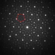
Precession electron diffraction
.gif)
Precession electron diffraction (PED), invented by Roger Vincent and
4D STEM
4D scanning transmission electron microscopy (4D STEM)[151] is a subset of scanning transmission electron microscopy (STEM) methods which uses a pixelated electron detector to capture a convergent beam electron diffraction (CBED) pattern at each scan location; see the main page for further information. This technique captures a 2 dimensional reciprocal space image associated with each scan point as the beam rasters across a 2 dimensional region in real space, hence the name 4D STEM. Its development was enabled by better STEM detectors and improvements in computational power. The technique has applications in diffraction contrast imaging, phase orientation and identification, strain mapping, and atomic resolution imaging among others; it has become very popular and rapidly evolving from about 2020 onwards.[151]
The name 4D STEM is common in literature, however it is known by other names: 4D STEM
Low-energy electron diffraction (LEED)


Low-energy electron diffraction (LEED) is a technique for the determination of the surface structure of
LEED may be used in one of two ways:[58][86]
- Qualitatively, where the diffraction pattern is recorded and analysis of the spot positions gives information on the symmetry of the surface structure. In the presence of an adsorbate the qualitative analysis may reveal information about the size and rotational alignment of the adsorbate unit cell with respect to the substrate unit cell.[58]
- Quantitatively, where the intensities of diffracted beams are recorded as a function of incident electron beam energy to generate the so-called I–V curves. By comparison with theoretical curves, these may provide accurate information on atomic positions on the surface.[86]
Reflection high-energy electron diffraction (RHEED)
.svg)

Reflection high energy electron diffraction (RHEED),
Gas electron diffraction

Gas electron diffraction (GED) can be used to determine the geometry of molecules in gases.[159] A gas carrying the molecules is exposed to the electron beam, which is diffracted by the molecules. Since the molecules are randomly oriented, the resulting diffraction pattern consists of broad concentric rings, see Figure 24. The diffraction intensity is a sum of several components such as background, atomic intensity or molecular intensity.[159]
In GED the diffraction intensities at a particular diffraction angle is described via a scattering variable defined as[160]


The most valuable information is carried by the intensity of molecular scattering , as it contains information about the distance between all pairs of atoms in the molecule. It is given by[160]
![{\displaystyle I_{m}(s)={\frac {K^{2}}{R^{2}}}I_{0}\sum _{i=1}^{N}\sum _{\stackrel {j=1}{i\neq j}}^{N}\left|f_{i}(s)\right|\left|f_{j}(s)\right|{\frac {\sin[s(r_{ij}-\kappa s^{2})]}{sr_{ij}}}e^{-(1/2l_{ij}s^{2})}\cos[\eta _{i}(s)-\eta _{i}(s)],}](https://wikimedia.org/api/rest_v1/media/math/render/svg/c1502d3b423fa3b7b59a79e49b0f2f9e3cd432a4)


Similar methods of analysis have also been applied to analyze electron diffraction data from liquids.[163][164][165]
In a scanning electron microscope

In a
Notes
- ^ a b Sometimes electron diffraction is defined similar to light or water wave diffraction, that is interference or bending of (electron) waves around the corners of an obstacle or through an aperture. With this definition the electrons are behaving as waves in a general sense, corresponding to a type of Fresnel diffraction. However, in every case where electron diffraction is used in practice the obstacles of relevance are atoms, so the general definition is not used herein.
- matter wavesfor more discussion.
- ^ Herein crystallographic conventions are used. Often in physics a plane wave is defined as . This changes some of the equations by a factor of , for instance appears instead of , but nothing significant.
- ^ a b c d Notations differ depending upon whether the source is crystallography, physics or other. In addition to for the reciprocal lattice vectors as used herein, sometimes are used. Less common, but still sometimes used, are for real space, and for reciprocal space. Also, sometimes reciprocal lattice vectors are written with capitals as not , and the length can differ by a factor of as mentioned above if is used for plane waves. (Different notations also exist for the wavevectors , or .) Similar notation differences can occur with aperiodic materials and superstructures. Furthermore, when dealing with surfaces as in Miller indicesare used for hexagonal systems even though only three are needed.


References
- ^ OCLC 247191522.
- ^ OCLC 1066178493.
- ^ ISBN 978-1-4020-1900-5
- ^ S2CID 250876999.
- ^ a b c d e f g h de Broglie, Louis Victor. "On the Theory of Quanta" (PDF). Foundation of Louis de Broglie (English translation by A.F. Kracklauer, 2004. ed.). Retrieved 25 February 2023.
- ^ ISBN 978-0-03-083993-1.
- ^ OCLC 2365578.
- ^ OCLC 656767858.
- ^ ISSN 0022-3719.
- ^ .
- ^ ISSN 0031-899X.
- ^ a b c d
ISBN 978-0-521-64222-4.
- ISBN 978-0-88029-751-6.
- ^ ISSN 0304-3886.
- PMID 18018443.
- ^ Michael Faraday (1838) "VIII. Experimental researches in electricity. — Thirteenth series.," Philosophical Transactions of the Royal Society of London, 128 : 125–168.
- ISSN 1941-5982.
- ^ ISBN 9780080577333
- ^ Goldstein, Eugen (1876). Monatsberichte der Königlich Preussischen Akademie der Wissenschaften zu Berlin (in German). The Academy. pp. 279–295, pp 286.
- ^ Whittaker, E.T. (1951). A History of the Theories of Aether and Electricity. Vol. 1. London: Nelson.
- ^ S2CID 122006529.
- ISSN 1941-5982.
- ^ Stoney, George Johnstone (1891). "Cause of Double Lines in Spectra". The Scientific Transactions of the Royal Dublin Society. 4. Dublin: 563, pp 583.
- ^ Einstein, Albert. Relativity: The Special and General Theory.
- ISSN 1941-5982.
- S2CID 4104602.
- ^ ISSN 0031-899X.
- ^ PMID 16587341.
- ^ PMID 16587378.
- S2CID 4122313.
- S2CID 98311959.
- S2CID 171025814.
- ^ .
- ^ S2CID 4121059– via Google Scholar.
- ^ a b Kikuchi, Seishi (1928). "Electron diffraction in single crystals". Japanese Journal of Physics. 5 (3061): 83–96.
- S2CID 9815364.
- S2CID 178706417.
- ISSN 0031-899X.
- ^ ISSN 0003-3804.
- ^ S2CID 186239132.
- ISSN 0021-8979.
- S2CID 195494352, retrieved 2023-02-24
- .
- ISSN 1941-5982.
- .
- ^ ISSN 0508-3443.
- ISBN 978-94-6252-528-3.
- PMID 14057363.
- ISBN 9780123810175, retrieved 2023-02-11.
- ^ "Max Knoll". AncientFaces. Retrieved 2023-09-26.
- ^ Rüdenberg, Reinhold. "Apparatus for producing images of objects". Patent Public Search Basic. Retrieved 24 February 2023.
- ^ Rüdenberg, Reinhold. "Apparatus for producing images of objects". Patent Public Search Basic. Retrieved 24 February 2023.
- S2CID 263996652.
- . Retrieved 2023-09-26.
- .
- S2CID 121097655.
- ISSN 0031-899X.
- ^ ISBN 978-3-540-16262-9.
- OCLC 7276396.
- ISSN 0003-6951.
- S2CID 123199621.
- ^ S2CID 94391285.
- ISSN 0365-110X.
- .
- ^ ISSN 0365-110X.
- S2CID 8016041.
- ISSN 0567-7394.
- ISSN 0025-5718.
- S2CID 20294294. Retrieved 2023-09-26.
- ^ .
- ^ .
- ^ S2CID 122890943.
- ^ ISSN 0021-8898.
- PMID 2681572.
- ^ ISSN 0108-7673.
- S2CID 98184340.
- S2CID 45473741.
- ^ a b c d Morniroli, Jean-Paul (2015). The atlas of electron diffraction zone axis patterns. Webpage and hardcopy.
{{cite book}}: CS1 maint: location missing publisher (link) - ^ ISBN 978-94-007-5579-6.
- ^ PMID 19910121.
- ^ PMID 23364455.
- ^ ISSN 0021-8979.
- ^ ISBN 9783540005452.
- S2CID 96851585.
- .
- ^ OCLC 1293917727.)
{{cite book}}: CS1 maint: location missing publisher (link - ^ OCLC 54529276.
- ^ ISSN 0034-6748.
- ^ PMID 12524196.
- ^ ISBN 978-0-07-085643-1.
- ISSN 0108-7673.
- ^ ISSN 0031-9015.
- ^ a b Howie, A (1962). "Discussion of K. Fujiwara's paper by M. J. Whelan". Journal of the Physical Society of Japan. 17(Supplement BII): 118.
- ^ "Bond Energies". Chemistry LibreTexts. 2013-10-02. Retrieved 2023-09-26.
- ISBN 9780080102412, retrieved 2023-02-11
- ISSN 0365-110X.
- ^ "Kevin Cowtan's Book of Fourier, University of York, UK". www.ysbl.york.ac.uk. Retrieved 2023-09-26.
- ^ S2CID 13112732.
- ^ "higher-order Laue zone (HOLZ) reflection | Glossary | JEOL Ltd". higher-order Laue zone (HOLZ) reflection | Glossary | JEOL Ltd. Retrieved 2023-10-02.
- ^ ISBN 978-4-431-56500-0, retrieved 2023-02-11
- S2CID 123349515.
- ^ ISSN 0031-9015.
- ^ S2CID 121465295.
- ^ S2CID 123122726.
- S2CID 8016041.
- ^ Metherell, A. J. (1975). Electron Microscopy in Materials Science: Part II. Commission of the European Communities. pp. 397–552.
- ISSN 0022-3719.
- ^ ISSN 0365-110X.
- .
- ^ ISSN 0021-9606.
- ^ ISSN 0567-7394.
- .
- ^ a b Faye, Jan (2019), "Copenhagen Interpretation of Quantum Mechanics", in Zalta, Edward N. (ed.), The Stanford Encyclopedia of Philosophy (Winter 2019 ed.), Metaphysics Research Lab, Stanford University, retrieved 2023-09-26
- ^ S2CID 243353224.
- ^ ISBN 9782901483052.
- ^ ISBN 978-0-12-813369-9.
- OCLC 1001251352.
- )
- )
- ISSN 0304-3991.
- ^ a b "Apertures, Electron Microscope Apertures". www.tedpella.com. Retrieved 2023-02-11.
- ISSN 0031-9015.
- ^ S2CID 20112743.
- PMID 17234347.
- PMID 19269095.
- ISSN 0031-8086.
- ISSN 0022-3093.
- ISSN 0031-9007.
- S2CID 16316238.
- ^ ISSN 0556-2805.
- ^ ISSN 0034-4885.
- ^ ISBN 978-1-4020-1900-5, retrieved 2023-03-24
- S2CID 233534909.
- ISSN 0305-4608.
- ^ "6.8: Ferro-, Ferri- and Antiferromagnetism". Chemistry LibreTexts. 2019-09-13. Retrieved 2023-09-26.
- S2CID 53137808.
- ISBN 978-3-540-00545-2.
- ^ ISSN 0734-2101.
- ISSN 1098-0121.
- ISSN 0031-9007.
- .
- S2CID 137476417.
- OCLC 45485010.
- PMID 34258017.
- PMID 15935917.
- S2CID 155224415.
- ^ Own, C. S.: PhD thesis, System Design and Verification of the Precession Electron Diffraction Technique, Northwestern University, 2005, http://www.numis.northwestern.edu/Research/Current/precession.shtml
- .
- .
- S2CID 52059939.
- ^ S2CID 263414171.
- ^ "4D STEM | Gatan, Inc". www.gatan.com. Retrieved 2022-03-13.
- PMID 29951584.
- .
- ISSN 0031-9007.
- PMID 20154691.
- ISSN 1466-8033.
- ^ OCLC 40857022.
- ^ ISSN 0005-9021.
- ^ S2CID 208256341.
- ^ .
- ^ ISSN 0904-213X.
- S2CID 4201332.
- ISSN 0026-8976.
- S2CID 227100401.
- S2CID 137281137.
- S2CID 137379846.
- S2CID 41385346.
- ^ OCLC 902763902.
Further reading
- John M., Cowley (1995). Diffraction physics. Elsevier. OCLC 247191522.. Contains extensive coverage of kinematical and other diffraction.
- Reimer, Ludwig (2013). Transmission Electron Microscopy : Physics of Image Formation and Microanalysis. Springer Berlin / Heidelberg. OCLC 1066178493. Large coverage of many different areas of electron microscopy with large numbers of references.
- Hirsch, P. B.; Howie, A.; Nicholson, R. B.; Pashley, D. W.; Whelan, M. J. (1965). Electron microscopy of thin crystals. London: Butterworths. OCLC 2365578., often called the bible of electron microscopy.
- Spence, J. C. H.; Zuo, J. M. (1992). Electron Microdiffraction. Boston, MA: Springer US. CBED
- Peng, L.-M.; Dudarev, S. L.; Whelan, M. J. (2011). High energy electron diffraction and microscopy. Oxford: Oxford University Press. OCLC 656767858.. Very extensive coverage of modern dynamical diffraction.
- Carter, C. Barry; Williams, David B.; Thomas, John M., eds. (2016). Transmission electron microscopy: diffraction, imaging, and spectrometry. Cham, Switzerland: Springer. ISBN 978-3-319-26649-7., a recent textbook with many images, stronger on experimental aspects.
- Edington, Jeffrey William (1977). Practical electron microscopy in materials science. Techbooks. OCLC 27997701., an older source for experimental details, albeit hard to find.