
Scanning electron microscope
This article needs additional citations for verification. (July 2023) |


A scanning electron microscope (SEM) is a type of electron microscope that produces images of a sample by scanning the surface with a focused beam of electrons. The electrons interact with atoms in the sample, producing various signals that contain information about the surface topography and composition of the sample. The electron beam is scanned in a raster scan pattern, and the position of the beam is combined with the intensity of the detected signal to produce an image. In the most common SEM mode, secondary electrons emitted by atoms excited by the electron beam are detected using a secondary electron detector (Everhart–Thornley detector). The number of secondary electrons that can be detected, and thus the signal intensity, depends, among other things, on specimen topography. Some SEMs can achieve resolutions better than 1 nanometer.
Specimens are observed in high vacuum in a conventional SEM, or in low vacuum or wet conditions in a variable pressure or environmental SEM, and at a wide range of cryogenic or elevated temperatures with specialized instruments.[1]
History
An account of the early history of scanning electron microscopy has been presented by McMullan.
Principles and capacities


The signals used by a SEM to produce an image result from interactions of the electron beam with atoms at various depths within the sample. Various types of signals are produced including secondary electrons (SE), reflected or back-scattered electrons (BSE), characteristic X-rays and light (cathodoluminescence) (CL), absorbed current (specimen current) and transmitted electrons. Secondary electron detectors are standard equipment in all SEMs, but it is rare for a single machine to have detectors for all other possible signals.[citation needed]
Secondary electrons have very low energies on the order of 50 eV, which limits their mean free path in solid matter. Consequently, SEs can only escape from the top few nanometers of the surface of a sample. The signal from secondary electrons tends to be highly localized at the point of impact of the primary electron beam, making it possible to collect images of the sample surface with a resolution of below 1 nm. Back-scattered electrons (BSE) are beam electrons that are reflected from the sample by elastic scattering. Since they have much higher energy than SEs, they emerge from deeper locations within the specimen and, consequently, the resolution of BSE images is less than SE images. However, BSE are often used in analytical SEM, along with the spectra made from the characteristic X-rays, because the intensity of the BSE signal is strongly related to the atomic number (Z) of the specimen. BSE images can provide information about the distribution, but not the identity, of different elements in the sample. In samples predominantly composed of light elements, such as biological specimens, BSE imaging can image colloidal gold immuno-labels of 5 or 10 nm diameter, which would otherwise be difficult or impossible to detect in secondary electron images.[14] Characteristic X-rays are emitted when the electron beam removes an inner shell electron from the sample, causing a higher-energy electron to fill the shell and release energy. The energy or wavelength of these characteristic X-rays can be measured by Energy-dispersive X-ray spectroscopy or Wavelength-dispersive X-ray spectroscopy and used to identify and measure the abundance of elements in the sample and map their distribution.
Due to the very narrow electron beam, SEM micrographs have a large
Sample preparation

SEM samples have to be small enough to fit on the specimen stage, and may need special preparation to increase their electrical conductivity and to stabilize them, so that they can withstand the high vacuum conditions and the high energy beam of electrons. Samples are generally mounted rigidly on a specimen holder or stub using a conductive adhesive. SEM is used extensively for defect analysis of semiconductor wafers, and manufacturers make instruments that can examine any part of a 300 mm semiconductor wafer. Many instruments have chambers that can tilt an object of that size to 45° and provide continuous 360° rotation.[citation needed]
Nonconductive specimens collect charge when scanned by the electron beam, and especially in secondary electron imaging mode, this causes scanning faults and other image artifacts. For conventional imaging in the SEM, specimens must be
An alternative to coating for some biological samples is to increase the bulk conductivity of the material by impregnation with osmium using variants of the OTO staining method (O-osmium tetroxide, T-thiocarbohydrazide, O-osmium).[16][17]
Nonconducting specimens may be imaged without coating using an environmental SEM (ESEM) or low-voltage mode of SEM operation. In ESEM instruments the specimen is placed in a relatively high-pressure chamber and the electron optical column is differentially pumped to keep vacuum adequately[clarification needed] low at the electron gun. The high-pressure region around the sample in the ESEM neutralizes charge and provides an amplification of the secondary electron signal.[citation needed] Low-voltage SEM is typically conducted in an instrument with a field emission guns (FEG) which is capable of producing high primary electron brightness and small spot size even at low accelerating potentials. To prevent charging of non-conductive specimens, operating conditions must be adjusted such that the incoming beam current is equal to sum of outgoing secondary and backscattered electron currents, a condition that is most often met at accelerating voltages of 0.3–4 kV.[citation needed]
Embedding in a resin with further polishing to a mirror-like finish can be used for both biological and materials specimens when imaging in backscattered electrons or when doing quantitative X-ray microanalysis.
The main preparation techniques are not required in the environmental SEM outlined below, but some biological specimens can benefit from fixation.
Biological samples
Conventionally, a SEM specimen is required to be completely dry, since the specimen chamber is under high vacuum. Hard, dry materials such as wood, bone, feathers, dried insects, or shells (including egg shells[18]) can be examined with little further treatment, but living cells and tissues and whole, soft-bodied organisms require chemical fixation to preserve and stabilize their structure.
Fixation is usually performed by incubation in a solution of a
The dry specimen is usually mounted on a specimen stub using an adhesive such as epoxy resin or electrically conductive double-sided adhesive tape, and
If the SEM is equipped with a cold stage for cryo microscopy, cryofixation may be used and low-temperature scanning electron microscopy performed on the cryogenically fixed specimens.[19] Cryo-fixed specimens may be cryo-fractured under vacuum in a special apparatus to reveal internal structure, sputter-coated and transferred onto the SEM cryo-stage while still frozen.[24] Low-temperature scanning electron microscopy (LT-SEM) is also applicable to the imaging of temperature-sensitive materials such as ice[25][26] and fats.[27]
Freeze-fracturing, freeze-etch or freeze-and-break is a preparation method particularly useful for examining lipid membranes and their incorporated proteins in "face on" view. The preparation method reveals the proteins embedded in the lipid bilayer.
Materials
Back-scattered electron imaging, quantitative X-ray analysis, and X-ray mapping of specimens often requires grinding and polishing the surfaces to an ultra-smooth surface. Specimens that undergo
Scanning process and image formation
This section needs additional citations for verification. (July 2023) |
.svg)
In a typical SEM, an electron beam is
The electron beam, which typically has an

When the primary electron beam interacts with the sample, the electrons lose energy by repeated random scattering and absorption within a teardrop-shaped volume of the specimen known as the interaction volume, which extends from less than 100 nm to approximately 5 µm into the surface. The size of the interaction volume depends on the electron's landing energy, the atomic number of the specimen, and the specimen's density. The energy exchange between the electron beam and the sample results in the reflection of high-energy electrons by elastic scattering, the emission of secondary electrons by

Magnification
Magnification in an SEM can be controlled over a range of about 6
Detection of secondary electrons
The most common imaging mode collects low-energy (<50 eV) secondary electrons that are ejected from conduction or valence bands of the specimen atoms by inelastic scattering interactions with beam electrons. Due to their low energy, these electrons originate from within a few
Detection of backscattered electrons

Top: backscattered electron analysis – composition
Bottom: secondary electron analysis – topography
Backscattered electrons (BSE) consist of high-energy electrons originating in the electron beam, that are reflected or back-scattered out of the specimen interaction volume by elastic scattering interactions with specimen atoms. Since heavy elements (high atomic number) backscatter electrons more strongly than light elements (low atomic number), and thus appear brighter in the image, BSEs are used to detect contrast between areas with different chemical compositions.[15] The Everhart–Thornley detector, which is normally positioned to one side of the specimen, is inefficient for the detection of backscattered electrons because few such electrons are emitted in the solid angle subtended by the detector, and because the positively biased detection grid has little ability to attract the higher energy BSE. Dedicated backscattered electron detectors are positioned above the sample in a "doughnut" type arrangement, concentric with the electron beam, maximizing the solid angle of collection. BSE detectors are usually either of scintillator or of semiconductor types. When all parts of the detector are used to collect electrons symmetrically about the beam, atomic number contrast is produced. However, strong topographic contrast is produced by collecting back-scattered electrons from one side above the specimen using an asymmetrical, directional BSE detector; the resulting contrast appears as illumination of the topography from that side. Semiconductor detectors can be made in radial segments that can be switched in or out to control the type of contrast produced and its directionality.
Backscattered electrons can also be used to form an electron backscatter diffraction (EBSD) image that can be used to determine the crystallographic structure of the specimen.
Beam-injection analysis of semiconductors
The nature of the SEM's probe, energetic electrons, makes it uniquely suited to examining the optical and electronic properties of semiconductor materials. The high-energy electrons from the SEM beam will inject
In a
Cathodoluminescence
Cathodoluminescence, the emission of light when atoms excited by high-energy electrons return to their ground state, is analogous to UV-induced fluorescence, and some materials such as zinc sulfide and some fluorescent dyes, exhibit both phenomena. Over the last decades, cathodoluminescence was most commonly experienced as the light emission from the inner surface of the cathode-ray tube in television sets and computer CRT monitors. In the SEM, CL detectors either collect all light emitted by the specimen or can analyse the wavelengths emitted by the specimen and display an emission spectrum or an image of the distribution of cathodoluminescence emitted by the specimen in real color.
X-ray microanalysis
Resolution of the SEM
An SEM is not a
Environmental SEM
Conventional SEM requires samples to be imaged under
The first commercial development of the ESEM in the late 1980s[32][33] allowed samples to be observed in low-pressure gaseous environments (e.g. 1–50 Torr or 0.1–6.7 kPa) and high relative humidity (up to 100%). This was made possible by the development of a secondary-electron detector[34][35] capable of operating in the presence of water vapour and by the use of pressure-limiting apertures with differential pumping in the path of the electron beam to separate the vacuum region (around the gun and lenses) from the sample chamber. The first commercial ESEMs were produced by the ElectroScan Corporation in USA in 1988. ElectroScan was taken over by Philips (who later sold their electron-optics division to FEI Company) in 1996.[36]
ESEM is especially useful for non-metallic and biological materials because coating with carbon or gold is unnecessary. Uncoated
Transmission SEM
The SEM can also be used in transmission mode by simply incorporating an appropriate detector below a thin specimen section.[38] Detectors are available for bright field, dark field, as well as segmented detectors for mid-field to high angle annular dark-field. Despite the difference in instrumentation, this technique is still commonly referred to as scanning transmission electron microscopy (STEM).
SEM in Forensic Science
The SEM is used often in Forensic Science for magnified analysis of microscopic things such as diatoms and gunshot residue. Because SEM is a nondestructive force on the sample, it can be used to analyze evidence without damaging it. The SEM shoots a beam of high energy electrons to the sample which bounce off of the sample without changing or destroying it. This is great when it comes to analyzing diatoms. When a person dies by drowning, they inhale the water which causes what is in the water (diatoms) to get in the blood stream, brain, kidneys, and more. These diatoms in the body can be magnified with the SEM to determine the type of diatoms which aid in understanding how and where the person died. By using the images produced by the SEM, forensic scientists can compare diatoms types to confirm the body of water a person died in.[39]
Gunshot residue (GSR) analysis can be done with many different analytical instruments,[40] but SEM is a common way to analyze inorganic compounds because of the way it can closely analyze the types of elements (mostly metals) through its three detectors: backscatter electron detector, secondary electron detector, and X-ray detector. GSR can be collected from the crime scene, victim, or shooter and analyzed with the SEM. This can help scientists determine proximity and or contact with the discharged firearm.[40]
Color in SEM
Electron microscopes do not naturally produce color images, as an SEM produces a single value per pixel; this value corresponds to the number of electrons received by the detector during a small period of time of the scanning when the beam is targeted to the (x, y) pixel position.
This single number is usually represented, for each pixel, by a grey level, forming a monochrome image.[41] However, several ways have been used to get color electron microscopy images.[42]
False color using a single detector
- On compositional images of flat surfaces (typically BSE):
The easiest way to get color is to associate to this single number an arbitrary color, using a
- On textured-surface images:
As an alternative to simply replacing each grey level by a color, a sample observed by an oblique beam allows researchers to create an approximative topography image (see further section "Photometric 3D rendering from a single SEM image"). Such topography can then be processed by 3D-rendering algorithms for a more natural rendering of the surface texture.
-
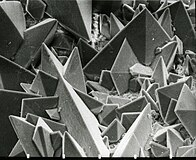 Surface of a kidney stone
 -
 The same after re-processing of the color from the estimated topography
 -
 SEM image of a diagenetically altered discoaster
 -
 The same image after similar colorization


SEM image coloring
Very often, published SEM images are artificially colored.[43] This may be done for aesthetic effect, to clarify structure or to add a realistic appearance to the sample and generally does not add information about the specimen.[44]
Coloring may be performed manually with photo-editing software, or semi-automatically with dedicated software using feature-detection or object-oriented segmentation.[45]
-
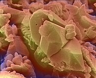
 SEM image of Cobaea scandens pollen
 -
 The same after semi-automatic coloring. Arbitrary colors help identifying the various elements of the structure
 -
 Colored SEM image of Tradescantia pollen and stamens
 -
 Colored SEM image of native gold and arsenopyrite crystal intergrowth


Color built using multiple electron detectors
In some configurations more information is gathered per pixel, often by the use of multiple detectors.[46]
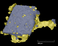
As a common example, secondary electron and backscattered electron detectors are superimposed and a color is assigned to each of the images captured by each detector,[47][48] with a result of a combined color image where colors are related to the density of the components. This method is known as density-dependent color SEM (DDC-SEM). Micrographs produced by DDC-SEM retain topographical information, which is better captured by the secondary electrons detector and combine it to the information about density, obtained by the backscattered electron detector.[49][50]
-
 DDC-SEM of calcified particle in cardiac tissue - Signal 1 : SE
 -
 Signal 2 : BSE
 -
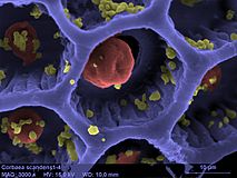
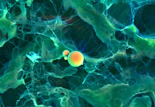 Colorized image obtained from the two previous. Density-dependent color scanning electron micrograph SEM (DDC-SEM) of cardiovascular calcification, showing in orange a calcium phosphate spherical particle (denser material) and, in green, the extracellular matrix (less dense material)
 -
 Same work with a larger view, part of a study on human cardiovascular tissue calcification


Analytical signals based on generated photons
Measurement of the energy of photons emitted from the specimen is a common method to get analytical capabilities. Examples are the
3D in SEM
SEMs do not naturally provide 3D images contrary to
3D SEM reconstruction from a stereo pair
- photogrammetry is the most metrologically accurate method to bring the third dimension to SEM images.[43] Contrary to photometric methods (next paragraph), photogrammetry calculates absolute heights using triangulation methods. The drawbacks are that it works only if there is a minimum texture, and it requires two images to be acquired from two different angles, which implies the use of a tilt stage. (Photogrammetry is a software operation that calculates the shift (or "disparity") for each pixel, between the left image and the right image of the same pair. Such disparity reflects the local height).
-
 An SEM stereo pair ofOstracoda) produced by tilting along the longitudinal axis.
 -
 From this pair of SEM images, the third dimension has been reconstructed by photogrammetry (using MountainsSEM software, see next image); then a series of 3D representations with different angles have been made and assembled into a GIF file to produce this animation.
 -
![3D surface reconstruction of a (Ra = 3 µm) roughness calibration sample (as used to calibrate profilometers), from 2 scanning electron microscope images tilted by 15° (top left). The calculation of the 3D model (bottom right) takes about 1.5 second[51] and the error on the Ra roughness value calculated is less than 0.5%.](//upload.wikimedia.org/wikipedia/commons/thumb/f/f5/3D_surface_reconstruction_from_2_scanning_electron_microscope_images.gif/337px-3D_surface_reconstruction_from_2_scanning_electron_microscope_images.gif) 3D surface reconstruction of a (Ra = 3 µm) roughness calibration sample (as used to calibrate profilometers), from 2 scanning electron microscope images tilted by 15° (top left). The calculation of the 3D model (bottom right) takes about 1.5 second[51] and the error on the Ra roughness value calculated is less than 0.5%.
3D surface reconstruction of a (Ra = 3 µm) roughness calibration sample (as used to calibrate profilometers), from 2 scanning electron microscope images tilted by 15° (top left). The calculation of the 3D model (bottom right) takes about 1.5 second[51] and the error on the Ra roughness value calculated is less than 0.5%.

.gif)
![3D surface reconstruction of a (Ra = 3 µm) roughness calibration sample (as used to calibrate profilometers), from 2 scanning electron microscope images tilted by 15° (top left). The calculation of the 3D model (bottom right) takes about 1.5 second[51] and the error on the Ra roughness value calculated is less than 0.5%.](/File:3D_surface_reconstruction_from_2_scanning_electron_microscope_images.gif)
Photometric 3D SEM reconstruction from a four-quadrant detector by "shape from shading"
This method typically uses a four-quadrant BSE detector (alternatively for one manufacturer, a 3-segment detector). The microscope produces four images of the same specimen at the same time, so no tilt of the sample is required. The method gives metrological 3D dimensions as far as the slope of the specimen remains reasonable.[43] Most SEM manufacturers now (2018) offer such a built-in or optional four-quadrant BSE detector, together with proprietary software to calculate a 3D image in real time.[52]
Other approaches use more sophisticated (and sometimes GPU-intensive) methods like the optimal estimation algorithm and offer much better results[53] at the cost of high demands on computing power.
In all instances, this approach works by integration of the slope, so vertical slopes and overhangs are ignored; for instance, if an entire sphere lies on a flat, little more than the upper hemisphere is seen emerging above the flat, resulting in wrong altitude of the sphere apex. The prominence of this effect depends on the angle of the BSE detectors with respect to the sample, but these detectors are usually situated around (and close to) the electron beam, so this effect is very common.
Photometric 3D rendering from a single SEM image
This method requires an SEM image obtained in oblique low angle lighting. The grey-level is then interpreted as the slope, and the slope integrated to restore the specimen topography. This method is interesting for visual enhancement and the detection of the shape and position of objects; however the vertical heights cannot usually be calibrated, contrary to other methods such as photogrammetry.[43]
-
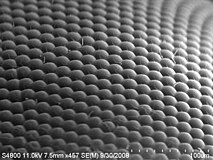 SEM image of a house fly compound eye surface at 450× magnification.
 -
 Detail of the previous image.
 -
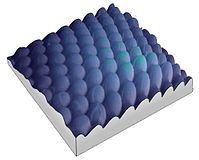 SEM 3D reconstruction from the previous usingshape from shadingalgorithms.
 -
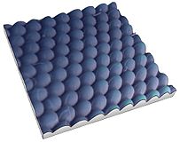 Same as the previous, but with lighting homogenized before applying the shape from shading algorithms.


Other types of 3D SEM reconstruction
- Inverse reconstruction using electron-material interactive models[54][55]
- Multi-Resolution reconstruction using single 2D File: High-quality 3D imaging may be an ultimate solution for revealing the complexities of any porous media, but acquiring them is costly and time-consuming. High-quality 2D SEM images, on the other hand, are widely available. Recently, a novel three-step, multiscale, multiresolution reconstruction method is presented that directly uses 2D images in order to develop 3D models. This method, based on a Shannon Entropy and conditional simulation, can be used for most of the available stationary materials and can build various stochastic 3D models just using a few thin sections.[56][57][58]
- Ion-abrasion SEM (IA-SEM) is a method of nanoscale 3D imaging that uses a focused beam of gallium to repeatedly abrade the specimen surface 20 nanometres at a time. Each exposed surface is then scanned to compile a 3D image.[59][60]
Applications of 3D SEM
One possible application is measuring the roughness of ice crystals. This method can combine variable-pressure environmental SEM and the 3D capabilities of the SEM to measure roughness on individual ice crystal facets, convert it into a computer model and run further statistical analysis on the model.[61] Other measurements include fractal dimension, examining fracture surface of metals, characterization of materials, corrosion measurement, and dimensional measurements at the nano scale (step height, volume, angle, flatness, bearing ratio, coplanarity, etc.).[citation needed]
SEM is also used by
Gallery of SEM images
The following are examples of images taken using an SEM.
-
 Colored SEM image of soybean cyst nematode and egg. The artificial coloring makes the image easier for non-specialists to view and understand the structures and surfaces revealed in micrographs.
 -
 Compound eye of Antarctic krill Euphausia superba. Arthropod eyes are a common subject in SEM micrographs due to the depth of focus that an SEM image can capture. Colored picture.
 -
 Ommatidia of Antarctic krill eye, a higher magnification of the krill's eye. SEMs cover a range from light microscopy up to the magnifications available with a TEM. Colored picture.
 -
 SEM image of normal circulating human blood. This is an older and noisy micrograph of a common subject for SEM micrographs: red blood cells.
 -
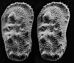
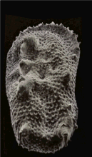
 SEM image of a hederelloid from the Devonian of Michigan (largest tube diameter is 0.75 mm). The SEM is used extensively for capturing detailed images of micro and macro fossils.
 -
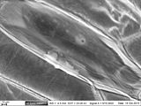
 Backscattered electron (BSE) image of an antimony-rich region in a fragment of ancient glass. Museums use SEMs for studying valuable artifacts in a nondestructive manner.
 -
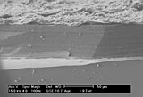 SEM image of the corrosion layer on the surface of an ancient glass fragment; note the laminar structure of the corrosion layer.
 -
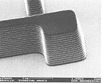 SEM image of a photoresist layer used in semiconductor manufacturing taken on a field emission SEM. These SEMs are important in the semiconductor industry for their high-resolution capabilities.
 -
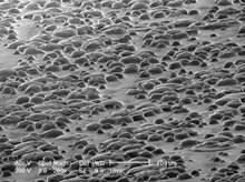
 SEM image of the surface of akidney stone showing tetragonal crystals of Weddellite(calcium oxalate dihydrate) emerging from the amorphous central part of the stone. Horizontal length of the picture represents 0.5 mm of the figured original.
 -
 Two images of the same depth hoar snow crystal, viewed through a light microscope (left) and as an SEM image (right). Note how the SEM image allows for clear perception of the fine structure details which are hard to fully make out in the light microscope image.
 -
 Epidermal cells from the inner surface of an onion flake. Beneath the shagreen-like cell walls one can see nuclei and small organelles floating in the cytoplasm. This BSE-image of a lanthanoid-stained sample was taken without prior fixation, dehydration, or sputtering.
 -
 SEM image of stomata on the lower surface of a leaf.


See also
- Applications for electron microscopy
- Electron microscopy
- Energy-dispersive X-ray spectroscopy
- Cathodoluminescence microscope
- Forensic engineering
- Forensic science
- List of materials analysis methods
- Microscopy
- Scanning helium microscopy
- Teeny Ted from Turnip Town (World's smallest book requires a scanning electron microscope to read).
- Transmission electron microscopy (TEM)
References
- ISBN 978-0470758748.
- PMC 2496789.
- ^ McMullan, D. (1988). "Von Ardenne and the scanning electron microscope". Proc Roy Microsc Soc. 23: 283–288.
- ^ Knoll, Max (1935). "Aufladepotentiel und Sekundäremission elektronenbestrahlter Körper". Zeitschrift für Technische Physik. 16: 467–475.
- ^ GB 511204, von Ardenne, Manfred, "Improvements in electron microscopes", published 1939-08-15
- ^ https://www.cambridge.org/core/services/aop-cambridge-core/content/view/07CA329CE1E1FF29442C48A64BC16C2F/S1551929500066402a.pdf/history-of-electron-microscopy-in-north-america.pdf
- S2CID 117900835.
- ^ von Ardenne, Manfred (1938). "Das Elektronen-Rastermikroskop. Praktische Ausführung". Zeitschrift für Technische Physik (in German). 19: 407–416.
- ^ Zworykin VA, Hillier J, Snyder RL (1942) A scanning electron microscope. ASTM Bull 117, 15–23.
- .
- ^ Oatley CW, Nixon WC, Pease RFW (1965) Scanning electron microscopy. Adv Electronics Electron Phys 21, 181–247.
- .
- ^ Wells OC (1957) The construction of a scanning electron microscope and its application to the study of fibres. PhD Dissertation, Cambridge University.
- ^ S2CID 42452027.
- ^ ISBN 978-0-306-40768-0.
- PMID 4165523.
- PMID 1103373.
- .
- ^ ISBN 978-0-12-318880-9.
- JSTOR 1604673.
- S2CID 100881495.
- .
- ISBN 9780763738747.
- PMID 18667640.
- ^ Wergin, W. P.; Erbe, E. F. (1994). "Snow crystals: capturing snow flakes for observation with the low-temperature scanning electron microscope". Scanning. 16 (Suppl. IV): IV88. Archived from the original on 17 February 2013. Retrieved 15 December 2012.
- S2CID 35513404.
- .
- ^ "Ultra-high Resolution Scanning Electron Microscope SU9000".
- .
- ^ Hitachi Launches World's Highest Resolution FE-SEM. Nanotech Now. 31 May 2011.
- PMID 25631998.
- ISBN 9780120146710.
- ^ US patent 4823006, Danilatos, Gerasimos D. and Lewis, George C., "Integrated electron optical/differential pumping/imaging signal detection system for an environmental scanning electron microscope", issued 18 April 1989
- ISBN 9780120146789.
- ^ US patent 4785182, Mancuso, James F.; Maxwell, William B. and Danilatos, Gerasimos D., "Secondary Electron Detector for Use in a Gaseous Atmosphere", issued 15 November 1988
- ^ History of Electron Microscopy 1990s Archived 4 March 2007 at archive.today. sfc.fr
- S2CID 21379512.
- ISBN 9780123942975.
- ^ "Forensic Applications of the Phenom Desktop Scanning Electron Microscope (SEM)". AZoNano.com. 21 February 2014. Retrieved 11 May 2023.
- ^ ISSN 2090-5939.
- ISBN 978-0521399401.
- ^ "Showing your true colors, 3D and color in electron microscopy in Lab News magazine".
- ^ .
- ^ "Introduction to Electron Microscopy" (PDF). FEI Company. p. 15. Retrieved 12 December 2012.
- ^ "Next Monday, Digital Surf to Launch Revolutionary SEM Image Colorization". AZO Materials. 22 January 2016. Retrieved 23 January 2016.
- .
- S2CID 96315383.
- .
- PMID 23603848.
- PMID 26056764.
- ^ Stereo SEM reconstruction using MountainsMap SEM version 7.4 on i7 2600 CPU at 3.4 GHz
- .
- .
- .
- .
- PMID 26560178.
- S2CID 20274015.
- S2CID 24307267.
- PMID 20399866.
- ^ "Multimedia Gallery - 3-D Imaging of Mammalian Cells With Ion-Abrasion SEM | NSF - National Science Foundation". www.nsf.gov.
- .
- S2CID 44166918.
External links
- General
- HowStuffWorks – How Scanning Electron Microscopes Work
- Learn to use an SEM – An online learning environment for people wanting to use an SEM. Provided by Microscopy Australia
- Virtual SEM – sparkler – an interactive simulation of a scanning electron microscope (SEM)
- Multichannel color SEM imaging – and with BSE
- Video on the scanning electron microscope, Karlsruhe University of Applied Sciences
- Animations and explanations on various types of microscopes including electron microscopes (Université Paris Sud)
- History
- Images
- Rippel Electron Microscope Facility Archived 19 March 2007 at the Wayback Machine Many dozens of (mostly biological) SEM images from Dartmouth College.
- Lanthanoid staining SEM images from Research Institute of Eye Diseases, Moscow.
| Basics |
| ||||||
|---|---|---|---|---|---|---|---|
| Electron interaction with matter | |||||||
| Instrumentation | |||||||
| Microscopes |
| ||||||
| Techniques |
| ||||||
| Others |
| ||||||