Harvard architecture
This article needs additional citations for verification. (March 2011) |

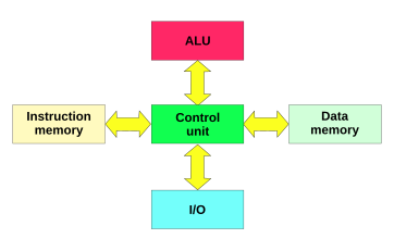
The Harvard architecture is a
The term is often stated as having originated from the
- 'The term "Harvard architecture" was coined decades later, in the context of microcontroller design' and only 'retrospectively applied to the Harvard machines and subsequently applied to RISC microprocessors with separated caches';
- 'The so-called "Harvard" and "von Neumann" architectures are often portrayed as a dichotomy, but the various devices labeled as the former have far more in common with the latter than they do with each other';
- 'In short [the Harvard architecture] isn't an architecture and didn't derive from work at Harvard'.
Modern processors appear to the user to be systems with von Neumann architectures, with the program code stored in the same
Harvard architecture is historically, and traditionally, split into two address spaces, but having three, i.e. two extra (and all accessed in each cycle) is also done,[2] while rare.
Memory details
In a Harvard architecture, there is no need to make the two memories share characteristics. In particular, the word width, timing, implementation technology, and memory address structure can differ. In some systems, instructions for pre-programmed tasks can be stored in read-only memory while data memory generally requires read-write memory. In some systems, there is much more instruction memory than data memory so instruction addresses are wider than data addresses.
Contrast with von Neumann architectures
In a system with a pure
Also, a Harvard architecture machine has distinct code and data address spaces: instruction address zero is not the same as data address zero. Instruction address zero might identify a twenty-four-bit value, while data address zero might indicate an eight-bit byte that is not part of that twenty-four-bit value.
Contrast with modified Harvard architecture
A
processors. It is sometimes loosely called a Harvard architecture, overlooking the fact that it is actually "modified".Another modification provides a pathway between the instruction memory (such as ROM or
Speed
In recent years, the speed of the CPU has grown many times in comparison to the access speed of the main memory. Care needs to be taken to reduce the number of times main memory is accessed in order to maintain performance. If, for instance, every instruction run in the CPU requires an access to memory, the computer gains nothing for increased CPU speed—a problem referred to as being
It is possible to make extremely fast memory, but this is only practical for small amounts of memory for cost, power and signal routing reasons. The solution is to provide a small amount of very fast memory known as a CPU cache which holds recently accessed data. As long as the data that the CPU needs is in the cache, the performance is much higher than it is when the CPU has to get the data from the main memory. On the other side, however, it may still be limited to storing repetitive programs or data and still has a storage size limitation, and other potential problems associated with it.[b]
Internal vs. external design
Modern high performance CPU chip designs incorporate aspects of both Harvard and von Neumann architecture. In particular, the "split cache" version of the modified Harvard architecture is very common. CPU cache memory is divided into an instruction cache and a data cache. Harvard architecture is used as the CPU accesses the cache. In the case of a cache miss, however, the data is retrieved from the main memory, which is not formally divided into separate instruction and data sections, although it may well have separate memory controllers used for concurrent access to RAM, ROM and (NOR) flash memory.
Thus, while a von Neumann architecture is visible in some contexts, such as when data and code come through the same memory controller, the hardware implementation gains the efficiencies of the Harvard architecture for cache accesses and at least some main memory accesses.
In addition, CPUs often have write buffers which let CPUs proceed after writes to non-cached regions. The von Neumann nature of memory is then visible when instructions are written as data by the CPU and software must ensure that the caches (data and instruction) and write buffer are synchronized before trying to execute those just-written instructions.
Modern uses of the Harvard architecture
The principal advantage of the pure Harvard architecture—simultaneous access to more than one memory system—has been reduced by modified Harvard processors using modern CPU cache systems. Relatively pure Harvard architecture machines are used mostly in applications where trade-offs, like the cost and power savings from omitting caches, outweigh the programming penalties from featuring distinct code and data address spaces.
- Texas Instruments TMS320C55x processors, for one example, feature multiple parallel data buses (two write, three read) and one instruction bus.
- AVR by Atmel Corp(now part of Microchip Technology).
Even in these cases, it is common to employ special instructions in order to access program memory as though it were data for read-only tables, or for reprogramming; those processors are modified Harvard architecture processors.
Notes
References
- S2CID 252018052.
- ^ "Kalimba DSP: User guide" (PDF). July 2006. p. 18. Retrieved 2022-09-23.
this is a three-bank Harvard architecture.
- ^ "386 vs. 030: the Crowded Fast Lane". Dr. Dobb's Journal, January 1988.
- OCLC 28966593.
- ^ "Embedded Systems Programming: Perils of the PC Cache". users.ece.cmu.edu. Archived from the original on January 15, 2020. Retrieved 2022-05-26.
