Transistor
A transistor is a
Most transistors are made from very pure silicon, and some from germanium, but certain other semiconductor materials are sometimes used. A transistor may have only one kind of charge carrier in a field-effect transistor, or may have two kinds of charge carriers in bipolar junction transistor devices. Compared with the vacuum tube, transistors are generally smaller and require less power to operate. Certain vacuum tubes have advantages over transistors at very high operating frequencies or high operating voltages, such as Traveling-wave tubes and Gyrotrons. Many types of transistors are made to standardized specifications by multiple manufacturers.
History
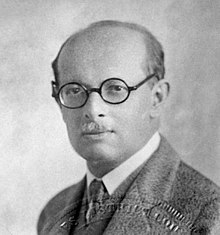
The
Bipolar transistors
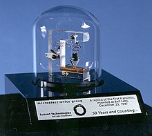
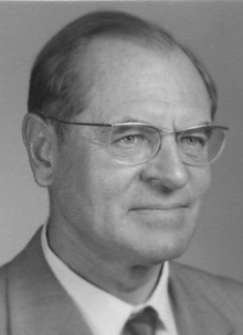
From November 17 to December 23, 1947,
Shockley's team initially attempted to build a field-effect transistor (FET) by trying to modulate the conductivity of a semiconductor, but was unsuccessful, mainly due to problems with the
In 1948, the point-contact transistor was independently invented by physicists
The first
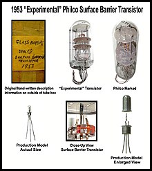
The first high-frequency transistor was the surface-barrier germanium transistor developed by Philco in 1953, capable of operating at frequencies up to 60 MHz.[30] They were made by etching depressions into an n-type germanium base from both sides with jets of indium(III) sulfate until it was a few ten-thousandths of an inch thick. Indium electroplated into the depressions formed the collector and emitter.[31][32]
AT&T first used transistors in telecommunications equipment in the No. 4A Toll Crossbar Switching System in 1953, for selecting trunk circuits from routing information encoded on translator cards.
The first prototype pocket
The first production all-transistor car radio was developed by Chrysler and Philco corporations and was announced in the April 28, 1955, edition of The Wall Street Journal. Chrysler made the Mopar model 914HR available as an option starting in fall 1955 for its new line of 1956 Chrysler and Imperial cars, which reached dealership showrooms on October 21, 1955.[39][40]
The
The first working silicon transistor was developed at Bell Labs on January 26, 1954, by
Field effect transistors
The basic principle of the field-effect transistor (FET) was first proposed by physicist Julius Edgar Lilienfeld when he filed a patent for a device similar to MESFET in 1926, and for an insulated-gate field-effect transistor in 1928.[11][47] The FET concept was later also theorized by engineer Oskar Heil in the 1930s and by William Shockley in the 1940s.
In 1945
In 1948, Bardeen patented the progenitor of MOSFET, an insulated-gate FET (IGFET) with an inversion layer. Bardeen's patent, and the concept of an inversion layer, forms the basis of CMOS technology today.[50]
MOSFET (MOS transistor)
In the early years of the
In 1957, Bell Labs engineer
Atalla and his Korean colleague
Importance
Because transistors are the key active components in practically all modern electronics, many people consider them one of the 20th century's greatest inventions.[2]
The invention of the first transistor at Bell Labs was named an
The MOSFET is by far the most widely used transistor, in applications ranging from
Although several companies each produce over a billion individually packaged (known as
The transistor's low cost, flexibility and reliability have made it ubiquitous. Transistorized mechatronic circuits have replaced electromechanical devices in controlling appliances and machinery. It is often easier and cheaper to use a standard microcontroller and write a computer program to carry out a control function than to design an equivalent mechanical system.
Simplified operation
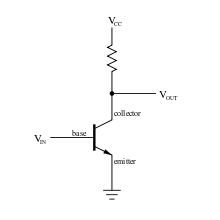
A transistor can use a small signal applied between one pair of its terminals to control a much larger signal at another pair of terminals, a property called gain. It can produce a stronger output signal, a voltage or current, proportional to a weaker input signal, acting as an amplifier. It can also be used as an electrically controlled switch, where the amount of current is determined by other circuit elements.[76]
There are two types of transistors, with slight differences in how they are used:
- A bipolar junction transistor (BJT)has terminals labeled base, collector and emitter. A small current at the base terminal, flowing between the base and the emitter, can control or switch a much larger current between the collector and emitter.
- A field-effect transistor (FET) has terminals labeled gate, source and drain. A voltage at the gate can control a current between source and drain.[77]
The top image in this section represents a typical bipolar transistor in a circuit. A charge flows between emitter and collector terminals depending on the current in the base. Because the base and emitter connections behave like a semiconductor diode, a voltage drop develops between them. The amount of this drop, determined by the transistor's material, is referred to as VBE.[77]
Transistor as a switch
Transistors are commonly used in
In a switching circuit, the goal is to simulate, as near as possible, the ideal switch having the properties of an open circuit when off, the short circuit when on, and an instantaneous transition between the two states. Parameters are chosen such that the "off" output is limited to leakage currents too small to affect connected circuitry, the resistance of the transistor in the "on" state is too small to affect circuitry, and the transition between the two states is fast enough not to have a detrimental effect.[77]
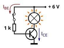
In a grounded-emitter transistor circuit, such as the light-switch circuit shown, as the base voltage rises, the emitter and collector currents rise exponentially. The collector voltage drops because of reduced resistance from the collector to the emitter. If the voltage difference between the collector and emitter were zero (or near zero), the collector current would be limited only by the load resistance (light bulb) and the supply voltage. This is called saturation because the current is flowing from collector to emitter freely. When saturated, the switch is said to be on.[78]
The use of bipolar transistors for switching applications requires biasing the transistor so that it operates between its cut-off region in the off-state and the saturation region (on). This requires sufficient base drive current. As the transistor provides current gain, it facilitates the switching of a relatively large current in the collector by a much smaller current into the base terminal. The ratio of these currents varies depending on the type of transistor, and even for a particular type, varies depending on the collector current. In the example of a light-switch circuit, as shown, the resistor is chosen to provide enough base current to ensure the transistor is saturated.[77] The base resistor value is calculated from the supply voltage, transistor C-E junction voltage drop, collector current, and amplification factor beta.[79]
Transistor as an amplifier

The
Various configurations of single transistor amplifiers are possible, with some providing current gain, some voltage gain, and some both.
From
Modern transistor audio amplifiers of up to a few hundred watts are common and relatively inexpensive.
Comparison with vacuum tubes
Before transistors were developed, vacuum (electron) tubes (or in the UK "thermionic valves" or just "valves") were the main active components in electronic equipment.
Advantages
The key advantages that have allowed transistors to replace vacuum tubes in most applications are
- No cathode heater (which produces the characteristic orange glow of tubes), reducing power consumption, eliminating delay as tube heaters warm up, and immune from cathode poisoningand depletion.
- Very small size and weight, reducing equipment size.
- Large numbers of extremely small transistors can be manufactured as a single integrated circuit.
- Low operating voltages compatible with batteries of only a few cells.
- Circuits with greater energy efficiency are usually possible. For low-power applications (for example, voltage amplification) in particular, energy consumption can be very much less than for tubes.
- Complementary devices available, providing design flexibility including complementary-symmetry circuits, not possible with vacuum tubes.
- Very low sensitivity to mechanical shock and vibration, providing physical ruggedness and virtually eliminating shock-induced spurious signals (for example, microphonics in audio applications).
- Not susceptible to breakage of a glass envelope, leakage, outgassing, and other physical damage.
Limitations
Transistors may have the following limitations:
- They lack the higher travelling wave tubesused as amplifiers in some satellites
- Transistors and other solid-state devices are susceptible to damage from very brief electrical and thermal events, including electrostatic discharge in handling. Vacuum tubes are electrically much more rugged.
- They are sensitive to radiation and cosmic rays (special radiation-hardened chips are used for spacecraft devices).
- In audio applications, transistors lack the lower-harmonic distortion – the so-called tube sound – which is characteristic of vacuum tubes, and is preferred by some.[80]
Types
Classification
This section needs additional citations for verification. (December 2020) |
Transistors are categorized by
- Structure: which?].
- Semiconductor material (dopants):
- The metalloids; germanium (first used in 1947) and silicon (first used in 1954)—in amorphous, polycrystalline and monocrystallineform.
- The compounds gallium arsenide (1966) and silicon carbide (1997).
- The silicon-germanium(1989)
- The allotrope of carbon graphene (research ongoing since 2004), etc. (see Semiconductor material).
- The
- PNP(BJTs), N-channel, P-channel (FETs).
- Maximum power rating: low, medium, high.
- Maximum operating frequency: low, medium, high, radio (RF), microwave frequency (the maximum effective frequency of a transistor in a common-emitter or common-source circuit is denoted by the term fT, an abbreviation for transition frequency—the frequency at which the transistor yields unity voltage gain)
- Application: switch, general purpose, audio, high voltage, super-beta, matched pair.
- Physical packaging: through-hole metal, through-hole plastic, surface mount, ball grid array, power modules (see Packaging).
- Amplification factor ).
- Working temperature: Extreme temperature transistors and traditional temperature transistors (−55 to 150 °C (−67 to 302 °F)). Extreme temperature transistors include high-temperature transistors (above 150 °C (302 °F)) and low-temperature transistors (below −55 °C (−67 °F)). The high-temperature transistors that operate thermally stable up to 250 °C (482 °F) can be developed by a general strategy of blending interpenetrating semi-crystalline conjugated polymers and high glass-transition temperature insulating polymers.[82]
Hence, a particular transistor may be described as silicon, surface-mount, BJT, NPN, low-power, high-frequency switch.
Mnemonics
Convenient
Field-effect transistor (FET)
The field-effect transistor, sometimes called a unipolar transistor, uses either electrons (in n-channel FET) or holes (in p-channel FET) for conduction. The four terminals of the FET are named source, gate, drain, and body (substrate). On most FETs, the body is connected to the source inside the package, and this will be assumed for the following description.
In a FET, the drain-to-source current flows via a conducting channel that connects the source region to the drain region. The conductivity is varied by the electric field that is produced when a voltage is applied between the gate and source terminals, hence the current flowing between the drain and source is controlled by the voltage applied between the gate and source. As the gate–source voltage (VGS) is increased, the drain–source current (IDS) increases exponentially for VGS below threshold, and then at a roughly quadratic rate: (IDS ∝ (VGS − VT)2, where VT is the threshold voltage at which drain current begins)
For low noise at narrow bandwidth, the higher input resistance of the FET is advantageous.
FETs are divided into two families: junction FET (JFET) and insulated gate FET (IGFET). The IGFET is more commonly known as a metal–oxide–semiconductor FET (MOSFET), reflecting its original construction from layers of metal (the gate), oxide (the insulation), and semiconductor. Unlike IGFETs, the JFET gate forms a p–n diode with the channel which lies between the source and drains. Functionally, this makes the n-channel JFET the solid-state equivalent of the vacuum tube triode which, similarly, forms a diode between its grid and cathode. Also, both devices operate in the depletion-mode, they both have a high input impedance, and they both conduct current under the control of an input voltage.
Metal–semiconductor FETs (
FETs are further divided into depletion-mode and enhancement-mode types, depending on whether the channel is turned on or off with zero gate-to-source voltage. For enhancement mode, the channel is off at zero bias, and a gate potential can "enhance" the conduction. For the depletion mode, the channel is on at zero bias, and a gate potential (of the opposite polarity) can "deplete" the channel, reducing conduction. For either mode, a more positive gate voltage corresponds to a higher current for n-channel devices and a lower current for p-channel devices. Nearly all JFETs are depletion-mode because the diode junctions would forward bias and conduct if they were enhancement-mode devices, while most IGFETs are enhancement-mode types.
Metal–oxide–semiconductor FET (MOSFET)
The metal–oxide–semiconductor field-effect transistor (
Bipolar junction transistor (BJT)
Bipolar transistors are so named because they conduct by using both majority and minority carriers. The bipolar junction transistor, the first type of transistor to be mass-produced, is a combination of two junction diodes and is formed of either a thin layer of p-type semiconductor sandwiched between two n-type semiconductors (an n–p–n transistor), or a thin layer of n-type semiconductor sandwiched between two p-type semiconductors (a p–n–p transistor). This construction produces two p–n junctions: a base-emitter junction and a base-collector junction, separated by a thin region of semiconductor known as the base region. (Two junction diodes wired together without sharing an intervening semiconducting region will not make a transistor.)
BJTs have three terminals, corresponding to the three layers of semiconductor—an emitter, a base, and a collector. They are useful in amplifiers because the currents at the emitter and collector are controllable by a relatively small base current.[86] In an n–p–n transistor operating in the active region, the emitter-base junction is forward-biased (electrons and holes recombine at the junction), and the base-collector junction is reverse-biased (electrons and holes are formed at, and move away from, the junction), and electrons are injected into the base region. Because the base is narrow, most of these electrons will diffuse into the reverse-biased base-collector junction and be swept into the collector; perhaps one-hundredth of the electrons will recombine in the base, which is the dominant mechanism in the base current. As well, as the base is lightly doped (in comparison to the emitter and collector regions), recombination rates are low, permitting more carriers to diffuse across the base region. By controlling the number of electrons that can leave the base, the number of electrons entering the collector can be controlled.[86] Collector current is approximately β (common-emitter current gain) times the base current. It is typically greater than 100 for small-signal transistors but can be smaller in transistors designed for high-power applications.
Unlike the field-effect transistor (see below), the BJT is a low-input-impedance device. Also, as the base-emitter voltage (VBE) is increased the base-emitter current and hence the collector-emitter current (ICE) increase exponentially according to the
Bipolar transistors can be made to conduct by exposure to light because the absorption of photons in the base region generates a photocurrent that acts as a base current; the collector current is approximately β times the photocurrent. Devices designed for this purpose have a transparent window in the package and are called
Usage of MOSFETs and BJTs
The
Other transistor types

- Field-effect transistor (FET):
- Metal–oxide–semiconductor field-effect transistor(MOSFET), where the gate is insulated by a shallow layer of insulator
- p-type MOS (PMOS)
- n-type MOS (NMOS)
- complementary MOS (CMOS)
- radiofrequencyamplification, reception
- Multi-gate field-effect transistor(MuGFET)
- Fin field-effect transistor (FinFET), source/drain region shapes fins on the silicon surface
- GAAFET, Similar to FinFET but nanowires are used instead of fins, the nanowires are stacked vertically and are surrounded on 4 sides by the gate
- MBCFET, a variant of GAAFET that uses horizontal nanosheets instead of nanowires, made by Samsung. Also known as RibbonFET (made by Intel) and as horizontal nanosheet transistor.
- Thin-film transistor (TFT), used in LCD and OLED displays, types include amorphous silicon, LTPS, LTPO and IGZO transistors
- non-volatile storage
- Power MOSFET, for power electronics
- lateral diffused MOS (LDMOS)
- Carbon nanotube field-effect transistor (CNFET, CNTFET), where the channel material is replaced by a carbon nanotube
- Ferroelectric field-effect transistor (Fe FET), uses ferroelectric materials
- Junction gate field-effect transistor(JFET), where the gate is insulated by a reverse-biased p–n junction
- Metal–semiconductor field-effect transistor(MESFET), similar to JFET with a Schottky junction instead of a p–n junction
- High-electron-mobility transistor (HEMT): GaN (Gallium Nitride), SiC (Silicon Carbide), Ga2O3 (Gallium Oxide), GaAs (Gallium Arsenide) transistors, MOSFETs, etc.
- Negative-Capacitance FET (NC-FET)
- Inverted-T field-effect transistor(ITFET)
- Fast-reverse epitaxial diode field-effect transistor(FREDFET)
- Organic field-effect transistor (OFET), in which the semiconductor is an organic compound
- Ballistic transistor (disambiguation)
- FETs used to sense the environment
- Bipolar junction transistor (BJT):
- Heterojunction bipolar transistor, up to several hundred GHz, common in modern ultrafast and RF circuits
- Schottky transistor
- avalanche transistor
- large-scale integration because this particular example is intended for power applications. Darlington transistorsare two BJTs connected together to provide a high current gain equal to the product of the current gains of the two transistors
- ASEA Brown Boveri (ABB) 5SNA2400E170100 ,[88]intended for three-phase power supplies, houses three n–p–n IGBTs in a case measuring 38 by 140 by 190 mm and weighing 1.5 kg. Each IGBT is rated at 1,700 volts and can handle 2,400 amperes
- Phototransistor.
- Emitter-switched bipolar transistor (ESBT) is a monolithic configuration of a high-voltage bipolar transistor and a low-voltage power MOSFET in cascode topology. It was introduced by STMicroelectronics in the 2000s,[89] and abandoned a few years later around 2012.[90]
- Multiple-emitter transistor, used in transistor–transistor logic and integrated current mirrors
- record player or radio front ends. Effectively, it is a very large number of transistors in parallel where, at the output, the signal is added constructively, but random noise is added only stochastically.[91]
- quantum tunnelingthrough a barrier.
- Diffusion transistor, formed by diffusing dopants into semiconductor substrate; can be both BJT and FET.
- Unijunction transistor, which can be used as a simple pulse generator. It comprises the main body of either p-type or n-type semiconductor with ohmic contacts at each end (terminals Base1 and Base2). A junction with the opposite semiconductor type is formed at a point along the length of the body for the third terminal (Emitter).
- Single-electron transistors (SET), consist of a gate island between two tunneling junctions. The tunneling current is controlled by a voltage applied to the gate through a capacitor.[92]
- Nanofluidic transistor, controls the movement of ions through sub-microscopic, water-filled channels.[93]
- Multigate devices:
- Tetrode transistor
- Pentode transistor
- Trigate transistor(prototype by Intel)
- oscillators.
- Junctionless nanowire transistor (JNT), uses a simple nanowire of silicon surrounded by an electrically isolated "wedding ring" that acts to gate the flow of electrons through the wire.
- Nanoscale vacuum-channel transistor, when in 2012, NASA and the National Nanofab Center in South Korea were reported to have built a prototype vacuum-channel transistor in only 150 nanometers in size, can be manufactured cheaply using standard silicon semiconductor processing, can operate at high speeds even in hostile environments, and could consume just as much power as a standard transistor.[94]
- Organic electrochemical transistor.
- Solaristor (from solar cell transistor), a two-terminal gate-less self-powered phototransistor.
- Germanium–Tin Transistor[95]
- Wood transistor[96][97]
- Paper transistor[98]
- Carbon-doped silicon-germanium (Si-Ge:C) transistor
- Diamond transistor[99]
- Aluminum nitride transistor[100]
- Super-lattice castellated field effect transistors[101]
Device identification
Three major identification standards are used for designating transistor devices. In each, the alphanumeric prefix provides clues to the type of the device.
Joint Electron Device Engineering Council (JEDEC)
The JEDEC part numbering scheme evolved in the 1960s in the United States. The JEDEC EIA-370 transistor device numbers usually start with 2N, indicating a three-terminal device. Dual-gate field-effect transistors are four-terminal devices, and begin with 3N. The prefix is followed by a two-, three- or four-digit number with no significance as to device properties, although early devices with low numbers tend to be germanium devices. For example, 2N3055 is a silicon n–p–n power transistor, 2N1301 is a p–n–p germanium switching transistor. A letter suffix, such as "A", is sometimes used to indicate a newer variant, but rarely gain groupings.
| Prefix | Type and usage |
|---|---|
| 1N | two-terminal device, such as diodes |
| 2N | three-terminal device, such as transistors or single-gate field-effect transistors |
| 3N | four-terminal device, such as dual-gate field-effect transistors |
Japanese Industrial Standard (JIS)
In Japan, the JIS semiconductor designation (|JIS-C-7012), labels transistor devices starting with 2S,[102] e.g., 2SD965, but sometimes the "2S" prefix is not marked on the package–a 2SD965 might only be marked D965 and a 2SC1815 might be listed by a supplier as simply C1815. This series sometimes has suffixes, such as R, O, BL, standing for red, orange, blue, etc., to denote variants, such as tighter hFE (gain) groupings.
| Prefix | Type and usage |
|---|---|
| 2SA | high-frequency p–n–p BJT |
| 2SB | audio-frequency p–n–p BJT |
| 2SC | high-frequency n–p–n BJT |
| 2SD | audio-frequency n–p–n BJT |
| 2SJ | P-channel FET (both JFET and MOSFET) |
| 2SK | N-channel FET (both JFET and MOSFET) |
European Electronic Component Manufacturers Association (EECA)
The European Electronic Component Manufacturers Association (EECA) uses a numbering scheme that was inherited from Pro Electron when it merged with EECA in 1983. This scheme begins with two letters: the first gives the semiconductor type (A for germanium, B for silicon, and C for materials like GaAs); the second letter denotes the intended use (A for diode, C for general-purpose transistor, etc.). A three-digit sequence number (or one letter and two digits, for industrial types) follows. With early devices this indicated the case type. Suffixes may be used, with a letter (e.g. "C" often means high hFE, such as in: BC549C[103]) or other codes may follow to show gain (e.g. BC327-25) or voltage rating (e.g. BUK854-800A[104]). The more common prefixes are:
| Prefix | Type and usage | Example | Equivalent | Reference |
|---|---|---|---|---|
| AC | AF transistor |
AC126 | NTE102A | |
| AD | Germanium, AF power transistor |
AD133 | NTE179 | |
| AF | Germanium, small-signal RF transistor |
AF117 | NTE160 | |
| AL | Germanium, RF power transistor |
ALZ10 | NTE100 | |
| AS | Germanium, switching transistor | ASY28 | NTE101 | |
| AU | Germanium, power switching transistor | AU103 | NTE127 | |
| BC | Silicon, small-signal transistor ("general purpose") | BC548 | 2N3904 | Datasheet |
| BD | Silicon, power transistor | BD139 | NTE375 | Datasheet |
| BF | Silicon, FET |
BF245 | NTE133 | Datasheet |
| BS | Silicon, switching transistor (BJT or MOSFET) | BS170 |
2N7000 | Datasheet |
| BL | Silicon, high frequency, high power (for transmitters) | BLW60 | NTE325 | Datasheet |
| BU | Silicon, high voltage (for CRT horizontal deflection circuits) | BU2520A | NTE2354 | Datasheet |
| CF | Gallium arsenide, small-signal microwave transistor (MESFET) | CF739 | — | Datasheet |
| CL | Gallium arsenide, microwave power transistor (FET) | CLY10 | — | Datasheet |
Proprietary
Manufacturers of devices may have their proprietary numbering system, for example
Military part numbers sometimes are assigned their codes, such as the British Military CV Naming System.
Manufacturers buying large numbers of similar parts may have them supplied with "house numbers", identifying a particular purchasing specification and not necessarily a device with a standardized registered number. For example, an HP part 1854,0053 is a (JEDEC) 2N2218 transistor[105][106] which is also assigned the CV number: CV7763[107]
Naming problems
With so many independent naming schemes, and the abbreviation of part numbers when printed on the devices, ambiguity sometimes occurs. For example, two different devices may be marked "J176" (one the J176 low-power JFET, the other the higher-powered MOSFET 2SJ176).
As older "through-hole" transistors are given surface-mount packaged counterparts, they tend to be assigned many different part numbers because manufacturers have their systems to cope with the variety in pinout arrangements and options for dual or matched n–p–n + p–n–p devices in one pack. So even when the original device (such as a 2N3904) may have been assigned by a standards authority, and well known by engineers over the years, the new versions are far from standardized in their naming.
Construction
This section needs additional citations for verification. (June 2021) |
Semiconductor material
| Semiconductor material |
Junction forward voltage @ 25 °C, V |
Electron mobility @ 25 °C, m2/(V·s) |
Hole mobility @ 25 °C, m2/(V·s) |
Max. junction temp., °C |
|---|---|---|---|---|
| Ge | 0.27 | 0.39 | 0.19 | 70 to 100 |
| Si | 0.71 | 0.14 | 0.05 | 150 to 200 |
| GaAs | 1.03 | 0.85 | 0.05 | 150 to 200 |
| Al–Si junction | 0.3 | — | — | 150 to 200 |
The first BJTs were made from
Rough parameters for the most common semiconductor materials used to make transistors are given in the adjacent table. These parameters will vary with an increase in temperature, electric field, impurity level, strain, and sundry other factors.
The junction forward voltage is the voltage applied to the emitter-base junction of a BJT to make the base conduct a specified current. The current increases exponentially as the junction forward voltage is increased. The values given in the table are typical for a current of 1 mA (the same values apply to semiconductor diodes). The lower the junction forward voltage the better, as this means that less power is required to "drive" the transistor. The junction forward voltage for a given current decreases with an increase in temperature. For a typical silicon junction, the change is −2.1 mV/°C.[108] In some circuits special compensating elements (sensistors) must be used to compensate for such changes.
The density of mobile carriers in the channel of a MOSFET is a function of the electric field forming the channel and of various other phenomena such as the impurity level in the channel. Some impurities, called dopants, are introduced deliberately in making a MOSFET, to control the MOSFET electrical behavior.
The
- Its maximum temperature is limited.
- It has relatively high leakage current.
- It cannot withstand high voltages.
- It is less suitable for fabricating integrated circuits.
Because the electron mobility is higher than the hole mobility for all semiconductor materials, a given bipolar
Maximum junction temperature values represent a cross-section taken from various manufacturers' datasheets. This temperature should not be exceeded or the transistor may be damaged.
Al–Si junction refers to the high-speed (aluminum-silicon) metal–semiconductor barrier diode, commonly known as a Schottky diode. This is included in the table because some silicon power IGFETs have a parasitic reverse Schottky diode formed between the source and drain as part of the fabrication process. This diode can be a nuisance, but sometimes it is used in the circuit.
Packaging

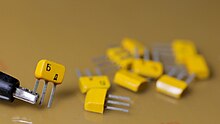
Discrete transistors can be individually packaged transistors or unpackaged transistor chips.
Transistors come in many different semiconductor packages (see image). The two main categories are through-hole (or leaded), and surface-mount, also known as surface-mount device (SMD). The ball grid array (BGA) is the latest surface-mount package. It has solder "balls" on the underside in place of leads. Because they are smaller and have shorter interconnections, SMDs have better high-frequency characteristics but lower power ratings.
Transistor packages are made of glass, metal, ceramic, or plastic. The package often dictates the power rating and frequency characteristics. Power transistors have larger packages that can be clamped to heat sinks for enhanced cooling. Additionally, most power transistors have the collector or drain physically connected to the metal enclosure. At the other extreme, some surface-mount microwave transistors are as small as grains of sand.
Often a given transistor type is available in several packages. Transistor packages are mainly standardized, but the assignment of a transistor's functions to the terminals is not: other transistor types can assign other functions to the package's terminals. Even for the same transistor type the terminal assignment can vary (normally indicated by a suffix letter to the part number, q.e. BC212L and BC212K).
Nowadays most transistors come in a wide range of SMT packages. In comparison, the list of available through-hole packages is relatively small. Here is a short list of the most common through-hole transistors packages in alphabetical order: ATV, E-line, MRT, HRT, SC-43, SC-72, TO-3, TO-18, TO-39, TO-92, TO-126, TO220, TO247, TO251, TO262, ZTX851.
Unpackaged transistor chips (die) may be assembled into hybrid devices.
Flexible transistors
Researchers have made several kinds of flexible transistors, including organic field-effect transistors.[110][111][112] Flexible transistors are useful in some kinds of flexible displays and other flexible electronics.
See also
- Band gap
- Digital electronics
- Diffused junction transistor
- Moore's law
- Optical transistor
- Magneto-Electric Spin-Orbit
- Nanoelectromechanical relay
- Semiconductor device modeling
- Transistor count
- Transistor model
- Transresistance
- Very Large Scale Integration
- Trancitor
References
- ^ "Transistor". Britannica. Retrieved January 12, 2021.
- ^ a b "A History of the Invention of the Transistor and Where It Will Lead Us" (PDF). IEEE JOURNAL OF SOLID-STATE CIRCUITS Vol 32 No 12. December 1997.
- ^ "1926 – Field Effect Semiconductor Device Concepts Patented". Computer History Museum. Archived from the original on March 22, 2016. Retrieved March 25, 2016.
- ^ "The Nobel Prize in Physics 1956". Nobelprize.org. Nobel Media AB. Archived from the original on December 16, 2014. Retrieved December 7, 2014.
- ^ a b "1960 - Metal Oxide Semiconductor (MOS) Transistor Demonstrated". The Silicon Engine. Computer History Museum.
- ^ ISBN 9783540342588.
- ^ a b c "Who Invented the Transistor?". Computer History Museum. December 4, 2013. Retrieved July 20, 2019.
- ISBN 9780262132480.
- ^ Lilienfeld, Julius Edgar (1927). Specification of electric current control mechanism patent application.
- ^ Vardalas, John (May 2003) Twists and Turns in the Development of the Transistor Archived January 8, 2015, at the Wayback Machine IEEE-USA Today's Engineer.
- ^ a b Lilienfeld, Julius Edgar, "Method and apparatus for controlling electric current" U.S. patent 1,745,175 January 28, 1930 (filed in Canada 1925-10-22, in US October 8, 1926).
- ^ "Method And Apparatus For Controlling Electric Currents". United States Patent and Trademark Office.
- ^ "Amplifier For Electric Currents". United States Patent and Trademark Office.
- ^ "Device For Controlling Electric Current". United States Patent and Trademark Office.
- ^ a b "Twists and Turns in the Development of the Transistor". Institute of Electrical and Electronics Engineers, Inc. Archived from the original on January 8, 2015.
- ^ Heil, Oskar, "Improvements in or relating to electrical amplifiers and other control arrangements and devices", Patent No. GB439457, European Patent Office, filed in Great Britain 1934-03-02, published December 6, 1935 (originally filed in Germany March 2, 1934).
- ^ "November 17 – December 23, 1947: Invention of the First Transistor". American Physical Society. Archived from the original on January 20, 2013.
- ^ Millman, S., ed. (1983). A History of Engineering and Science in the Bell System, Physical Science (1925–1980). AT&T Bell Laboratories. p. 102.
- ISBN 978-0-7394-5670-5.
- ^ "transistor". American Heritage Dictionary (3rd ed.). Boston: Houghton Mifflin. 1992.
- ^ "The Nobel Prize in Physics 1956". nobelprize.org. Archived from the original on March 12, 2007.
- ^ S2CID 38161381.
- S2CID 108955928. Archived from the original on October 21, 2021.)
{{cite book}}:|journal=ignored (help - ISBN 9783527340538.
- ^ FR 1010427 H. F. Mataré / H. Welker / Westinghouse: "Nouveau sytème crystallin à plusieur électrodes réalisant des relais de effects électroniques" filed on August 13, 1948
- ^ US 2673948 H. F. Mataré / H. Welker / Westinghouse, "Crystal device for controlling electric currents by means of a solid semiconductor" French priority August 13, 1948
- ^ "1948, The European Transistor Invention". Computer History Museum. Archived from the original on September 29, 2012.
- ^ "1951: First Grown-Junction Transistors Fabricated | The Silicon Engine | Computer History Museum". www.computerhistory.org. Archived from the original on April 4, 2017.
- ^ "A Working Junction Transistor". PBS. Archived from the original on July 3, 2017. Retrieved September 17, 2017.
- S2CID 51652314.
- ^ The Wall Street Journal, December 4, 1953, page 4, Article "Philco Claims Its Transistor Outperforms Others Now In Use"
- ^ Electronics magazine, January 1954, Article "Electroplated Transistors Announced"
- ^ P. Mallery, Transistors and Their Circuits in the 4A Toll Crossbar Switching System, AIEE Transactions, September 1953, p.388
- ^ 1953 Foreign Commerce Weekly; Volume 49; pp.23
- ^ "Der deutsche Erfinder des Transistors – Nachrichten Welt Print – DIE WELT". Die Welt. Welt.de. November 23, 2011. Archived from the original on May 15, 2016. Retrieved May 1, 2016.
- ^ "Regency TR-1 Transistor Radio History". Archived from the original on October 21, 2004. Retrieved April 10, 2006.
- ^ "The Regency TR-1 Family". Archived from the original on April 27, 2017. Retrieved April 10, 2017.
- ^ "Regency manufacturer in USA, radio technology from United St". Archived from the original on April 10, 2017. Retrieved April 10, 2017.
- ^ Wall Street Journal, "Chrysler Promises Car Radio With Transistors Instead of Tubes in '56", April 28, 1955, page 1
- ^ "FCA North America - Historical Timeline 1950-1959". www.fcanorthamerica.com. Archived from the original on April 2, 2015. Retrieved December 5, 2017.
- ISBN 978-0313398636.
- ^ Snook, Chris J. (November 29, 2017). "The 7 Step Formula Sony Used to Get Back On Top After a Lost Decade". Inc.
- ^ Kozinsky, Sieva (January 8, 2014). "Education and the Innovator's Dilemma". Wired. Retrieved October 14, 2019.
- ^ Riordan, Michael (May 2004). "The Lost History of the Transistor". IEEE Spectrum: 48–49. Archived from the original on May 31, 2015.
- ISBN 3-540-40546-1.
- ISBN 0-07-145951-0.
- ^ Lilienfeld, Julius Edgar, "Device for controlling electric current" U.S. patent 1,900,018 March 7, 1933 (filed in US March 28, 1928).
- ISBN 978-3-642-13884-3.
- ^ Junction Field-Effect Devices, Semiconductor Devices for Power Conditioning, 1982.
- .
- ^ ISBN 9780470508923.
- ^ a b c "Martin Atalla in Inventors Hall of Fame, 2009". Retrieved June 21, 2013.
- ^ a b "Dawon Kahng". National Inventors Hall of Fame. Retrieved June 27, 2019.
- ISBN 9783540342588.
- OCLC 634332043.
- S2CID 29105721. Archived from the original(PDF) on July 19, 2019.
- EETimes. December 12, 2018. Retrieved July 18, 2019.
- JSTOR 24923169.
- ^ "1963: Complementary MOS Circuit Configuration is Invented". Computer History Museum. Retrieved July 6, 2019.
- ^ D. Kahng and S. M. Sze, "A floating gate and its application to memory devices", The Bell System Technical Journal, vol. 46, no. 4, 1967, pp. 1288–1295
- ISBN 9780387717517.
- ISSN 0038-1101.
- ^ "IEEE Andrew S. Grove Award Recipients". IEEE Andrew S. Grove Award. Institute of Electrical and Electronics Engineers. Retrieved July 4, 2019.
- ^ "The Breakthrough Advantage for FPGAs with Tri-Gate Technology" (PDF). Intel. 2014. Retrieved July 4, 2019.
- ^ "Milestones:Invention of the First Transistor at Bell Telephone Laboratories, Inc., 1947". IEEE Global History Network. IEEE. Archived from the original on October 8, 2011. Retrieved August 3, 2011.
- ^ "List of IEEE Milestones". December 9, 2020.
- ^ a b "Remarks by Director Iancu at the 2019 International Intellectual Property Conference". United States Patent and Trademark Office. June 10, 2019. Retrieved July 20, 2019.
- ISBN 9780130470652.
- S2CID 25283342.
In the field of electronics, the planar Si metal–oxide–semiconductor field-effect transistor (MOSFET) is perhaps the most important invention.
- ISBN 9789814613750.
- ^ a b "Triumph of the MOS Transistor". YouTube. Computer History Museum. August 6, 2010. Archived from the original on December 11, 2021. Retrieved July 21, 2019.
- ^ "The most manufactured human artifact in history". Computer History. April 2, 2018. Retrieved January 21, 2021.
- ^ FETs/MOSFETs: Smaller apps push up surface-mount supply. globalsources.com (April 18, 2007)
- ^ "Introducing M1 Pro and M1 Max: the most powerful chips Apple has ever built - Apple". www.apple.com. Retrieved October 20, 2022.
- ISBN 978-3-319-41198-9.
- ISBN 978-1-5124-2146-0.
- ^ ISBN 978-1-139-48467-1.
- ISBN 978-0-511-07668-8.
- ^ "Transistor Base Resistor Calculator". January 27, 2012.
- ^ van der Veen, M. (2005). "Universal system and output transformer for valve amplifiers" (PDF). 118th AES Convention, Barcelona, Spain. Archived (PDF) from the original on December 29, 2009.
- ^ "Transistor Example". Archived from the original on February 8, 2008. 071003 bcae1.com
- PMID 30523104.
- ISBN 978-0-521-37095-0.
- ^
Sansen, W. M. C. (2006). Analog design essentials. New York, Berlin: Springer. p. §0152, p. 28. ISBN 978-0-387-25746-4.
- ^ a b "13 Sextillion & Counting: The Long & Winding Road to the Most Frequently Manufactured Human Artifact in History". Computer History Museum. April 2, 2018. Retrieved July 28, 2019.
- ^ ISBN 978-0-13-822023-5.
- ^ "MOSFET DIFFERENTIAL AMPLIFIER" (PDF). Boston University. Retrieved August 10, 2019.
- ^ "IGBT Module 5SNA 2400E170100" (PDF). Archived from the original (PDF) on April 26, 2012. Retrieved June 30, 2012.
- .
- ^ STMicroelectronics. "ESBTs". www.st.com. Retrieved February 17, 2019.
ST no longer offers these components, this web page is empty, and datasheets are obsoletes
- ISBN 0792390962.
- ^ "Single Electron Transistors". Snow.stanford.edu. Archived from the original on April 26, 2012. Retrieved June 30, 2012.
- ^ Sanders, Robert (June 28, 2005). "Nanofluidic transistor, the basis of future chemical processors". Berkeley.edu. Archived from the original on July 2, 2012. Retrieved June 30, 2012.
- ^ "The return of the vacuum tube?". Gizmag.com. May 28, 2012. Archived from the original on April 14, 2016. Retrieved May 1, 2016.
- ^ "New Type of Transistor from a Germanium–Tin Alloy Developed". April 28, 2023.
- ^ "Timber! The World's First Wooden Transistor - IEEE Spectrum".
- ^ "Boffins claim to create the world's first wooden transistor".
- ^ "Paper Transistor - IEEE Spectrum". spectrum.ieee.org.
- ^ "This Diamond Transistor Is Still Raw, But Its Future Looks Bright - IEEE Spectrum". spectrum.ieee.org.
- ^ "The New, New Transistor - IEEE Spectrum". spectrum.ieee.org.
- ^ Staff, The SE (February 23, 2024). "Chip Industry Week In Review". Semiconductor Engineering.
- ^ "Transistor Data". Clivetec.0catch.com. Archived from the original on April 26, 2016. Retrieved May 1, 2016.
- ^ "Datasheet for BC549, with A, B and C gain groupings" (PDF). Fairchild Semiconductor. Archived (PDF) from the original on April 7, 2012. Retrieved June 30, 2012.
- ^ "Datasheet for BUK854-800A (800volt IGBT)" (PDF). Archived (PDF) from the original on April 15, 2012. Retrieved June 30, 2012.
- ^ "Richard Freeman's HP Part numbers Crossreference". Hpmuseum.org. Archived from the original on June 5, 2012. Retrieved June 30, 2012.
- ^ "Transistor–Diode Cross Reference – H.P. Part Numbers to JEDEC (pdf)" (PDF). Archived (PDF) from the original on May 8, 2016. Retrieved May 1, 2016.
- ^ "CV Device Cross-reference by Andy Lake". Qsl.net. Archived from the original on January 21, 2012. Retrieved June 30, 2012.
- ISBN 978-0-19-514251-8.
- ^ ISBN 9780387339139.
A hybrid circuit is defined as an assembly containing both active semiconductor devices (packaged and unpackaged)
- PMID 24018904.
- S2CID 109292175.
- S2CID 205446925.
Further reading
- Books
- ISBN 978-0521809269.)
{{cite book}}: CS1 maint: multiple names: authors list (link - Amos SW, James MR (1999). Principles of Transistor Circuits. Butterworth-Heinemann. ISBN 978-0-7506-4427-3.
- Riordan, Michael & Hoddeson, Lillian (1998). Crystal Fire. W.W Norton & Company Limited. ISBN 978-0-393-31851-7. The invention of the transistor & the birth of the information age
- Warnes, Lionel (1998). Analogue and Digital Electronics. Macmillan Press Ltd. ISBN 978-0-333-65820-8.
- The Power Transistor - Temperature and Heat Transfer; 1st Ed; John McWane, Dana Roberts, Malcom Smith; McGraw-Hill; 82 pages; 1975; ISBN 978-0-07-001729-0. (archive)
- Transistor Circuit Analysis - Theory and Solutions to 235 Problems; 2nd Ed; Alfred Gronner; Simon and Schuster; 244 pages; 1970. (archive)
- Transistor Physics and Circuits; R.L. Riddle and M.P. Ristenbatt; Prentice-Hall; 1957.
- Periodicals
- Michael Riordan (2005). "How Europe Missed the Transistor". IEEE Spectrum. 42 (11): 52–57. S2CID 34953819. Archived from the originalon February 14, 2008.
- "Herbert F. Mataré, An Inventor of the Transistor has his moment". The New York Times. February 24, 2003. Archived from the original on June 23, 2009.
- Bacon, W. Stevenson (1968). "The Transistor's 20th Anniversary: How Germanium And A Bit of Wire Changed The World". Popular Science. 192 (6): 80–84. ISSN 0161-7370.
- Databooks
- Discrete Databook; 1985; Fairchild (now ON Semiconductor)
- Small-Signal Semiconductors Databook, 1987; Motorola (now ON semiconductor)
- Discrete Power Devices Databook; 1982; SGS (now STMicroelectronics)
- Discrete Databook; 1978; National Semiconductor (now Texas Instruments)
External links
- BBC: Building the digital age photo history of transistors
- The Bell Systems Memorial on Transistors
- IEEE Global History Network, The Transistor and Portable Electronics. All about the history of transistors and integrated circuits.
- This Month in Physics History: November 17 to December 23, 1947: Invention of the First Transistor. From the American Physical Society
- Transistor | Definition & Uses | Britannica "Transistor" at Encyclopædia Britannica


